IPC-7095C-2013.pdf - 第116页
component solder ball, or during the reflow attachment process of the ball to the component. V oids can also form near the PCB to ball interface during BGA to PCB attach- ment. These voids are typically formed during the …

Another approach is to place a low cost in-circuit tester
near the end of the assembly line and use it as a manufac-
turing defect analyzer (MDA). Boards are tested immedi-
ately after the components are placed and soldered. Prob-
lems are quickly relayed back to manufacturing so
corrective action can take place while the product is being
assembled.
ICT can be supplemented by a complete functional test at
the end of assembly. This test for product functionality can,
depending on type of product and the acceptability require-
ments, be as simple as a ‘‘go/no-go’’ test or as complex as
a complete exercising of all circuit functionality. FT is used
to detect device faults on the assembly at speed. With the
higher temperatures on lead-free solder pastes, there may
be an increase in oxidized test lands or test vias. Typically,
with tin/lead alloys you may print and reflow solder pastes
to provide a soldered test point for the ICT probes. Lead-
free solder pastes do not wet as well and may cause issues
with ICT. It is recommended to run a quick experiment
during the development stage of the process to understand
the impact of lead-free solder pastes on this process.
7.4.2 Test Coverage Given the current complexity in
electronic assemblies, the level of ‘‘coverage’’ of test has
become an industry issue. The more complex a board or
assembly, the more difficult it is to fully test. Indeed, it may
be difficult to test even a reasonable portion of the assem-
bly in a reasonable, i.e., cost effective, period of time.
While test of an assembly may be aided by incorporating
test into the silicon devices, this strategy is not applicable
to bare boards. Thus the challenge of test is to provide test
coverage at a high level of confidence within a reasonable
period of time.
An effective process monitoring system consists of over-
lapping tools that create a large bandwidth of coverage.
Multiple tools and methods are required since there is not
one single tool or method that provides the desired cover-
age. Optical inspection, X-ray, SAM, ICT and FT are
examples of overlapping coverage. These verification
methods should be used to monitor products and process;
they should not be used solely to screen and separate good
and bad product.
7.4.3 Burn-In Testing Burn-in is an operational and
environmental test of the complete assembly at the upper
limits of the application. This test typically finds more
component related problems than solder joint defects. The
use of burn-in testing is still in use for component evalua-
tion. Burn-in on electronic assembly is decreasing in favor
of some form of accelerated test exposure to screen out
marginal results.
7.4.4 Product Screening Tests Environmental stress
screening (ESS) is used to screen ongoing production for
poor product quality and latent defects. The purpose of
ESS is to accelerate the latent defects to actual failures,
thus eliminating these latent defects from causing failures
in the field. Care must be taken that the ESS procedures are
not sufficiently severe to damage good product and produce
new latent defects. Solder fatigue life on BGAs shall be
evaluated on the thermal cycling of these ESS tests, other
tests, and the operating life thermal environments.
7.5 Void Identification The degree of voids permitted in
the BGA assembly attachment process and the impact on
reliability is of interest to members of the electronics
industry. The detailed requirements for end product accep-
tance shall be in accordance with J-STD-001; workman-
ship requirements shall follow the requirements of IPC-A-
610.
This section establishes the useful process development
and maintenance criteria to minimize occurrence of voids.
Current industry data suggests that voids in the solder joint
are not a reliability concern. In fact, the appearance of a
void after assembly reflow is an indicator that the reflow
process has taken place and the BGA ball has changed
characteristics. However, the aim of the process engineer
should be to minimize voids because excessive frequency
of voids may be an indication that the manufacturing
parameters need to be adjusted. Two reported causes of
voids are trapped flux that has not had enough time to be
released from the solder paste, and contaminants on
improperly cleaned circuit boards. Voids appear as a lighter
area inside the solder balls and are usually found randomly
throughout the package. Some X-ray systems can distort
the size of voids through blooming. It is possible to accu-
rately measure the true volume of a void but the procedure
can be involved and requires a known reference for radio-
metric calibration of the X-ray film or detector.
The size of BGA voids is not always the best criteria for
determining fatigue life of the solder joint. Large macro
process voids away from the solder joint to the component
land interface may not be a problem, whereas small voids
at the interface can become the criteria for fracture once a
crack starts. The location of the voids within the solder
joint is a bigger issue than the size and number of voids. In
most cases the effort is better spent on identifying and
eliminating the cause of the voids by following the design
and reflow profiles suggested in this document.
7.5.1 Sources of Voids There can be voids in a BGA
solder ball, in the solder joint to BGA interface, or in the
solder joint to PCB interface. Various sources or reasons
can be responsible for these voids.
Voids in the solder joints can be carried over from original
voids in solder balls, which could be the result of the ball
manufacturing process. Voids can be induced into the
reflowed solder joint by either the voids in the original
January 2013 IPC-7095C
101
Copyright IPC-Association Connecting Electronics Industries
Provided by IHS under license with IPC
Not for Resale
No reproduction or networking permitted without license from IHS
--`,,```,,,,````-`-`,,`,,`,`,,`---
component solder ball, or during the reflow attachment
process of the ball to the component. Voids can also form
near the PCB to ball interface during BGA to PCB attach-
ment. These voids are typically formed during the reflow
soldering process by flux volatiles trapped during the
solidification of the molten solder. The source of flux vola-
tiles can be either from applied flux itself (typically
rework), or flux which is one of the constituents of the sol-
der paste used in the reflow assembly process.
Solder joint voids are caused by solidification shrinkage,
moisture, and flux volatilization as defined in the follow-
ing:
• Shrinkage – Metal contraction during solidification will
result in some voids. The interior of a solder joint is the
last part of the joint to solidify so you expect it to have a
void.
• Moisture and contaminates supply gases that can be
trapped.
• Flux in the paste degrades and becomes gaseous during
ramp-up in the reflow oven. On a BGA the gases are
tightly sandwiched between two surfaces and the voids
that occur typically rise to the top of the solder joint. A
high ramp rate can cause more voiding by not allowing
time for void migration out of the joint (ramp rate
example, 75 vs. 60°C/minute).
• Paste flux to attach PBGAs tends to produce fewer voids
than with solder paste.
• Too much flux added during the rework process can cause
voids.
• Proper oven profile and clean parts can reduce solder
voids.
In addition to voids formed from via-in-pad construction
(see 6.3.5), some voids are detected in the middle to top
(ball/ BGA interface) of the reflowed solder joint. This is
expected because the trapped air bubble and the vaporized
flux, which is applied to the PCB BGA lands, rises during
the reflow profile. This occurs when the applied solder
paste and the BGA’s collapsible eutectic solder ball(s) melt
together during the reflow profile, typically 210-220°C
peak temperature for tin/lead and 235-245°C for lead free.
The metallurgical composition and surface roughness of an
incoming component ball can also add to ball void cre-
ation.
If the reflow profile cycle doesn’t allow sufficient time for
either the trapped air or vaporized flux to escape, a void is
formed as the molten solder solidifies in the cool down
area of the reflow profile. Therefore, the development of
the reflow profile is extremely important as a contributor to
the formation of voids. It is important to work with your
solder paste manufacturer to establish the reflow profile for
the solder paste formulation you are going to implement.
Voids in solder joints are not new. Voids can be detected
under leaded components when using X-ray equipment;
however, leaded component solder joints were historically
visually inspected, not X-rayed, and therefore hidden voids
were never detected. BGA suppliers should X-ray compo-
nents before and after the J-STD-002 Surface Mount Simu-
lation Test (Test S) is run to reveal anomalies that may lead
to solderability problems.
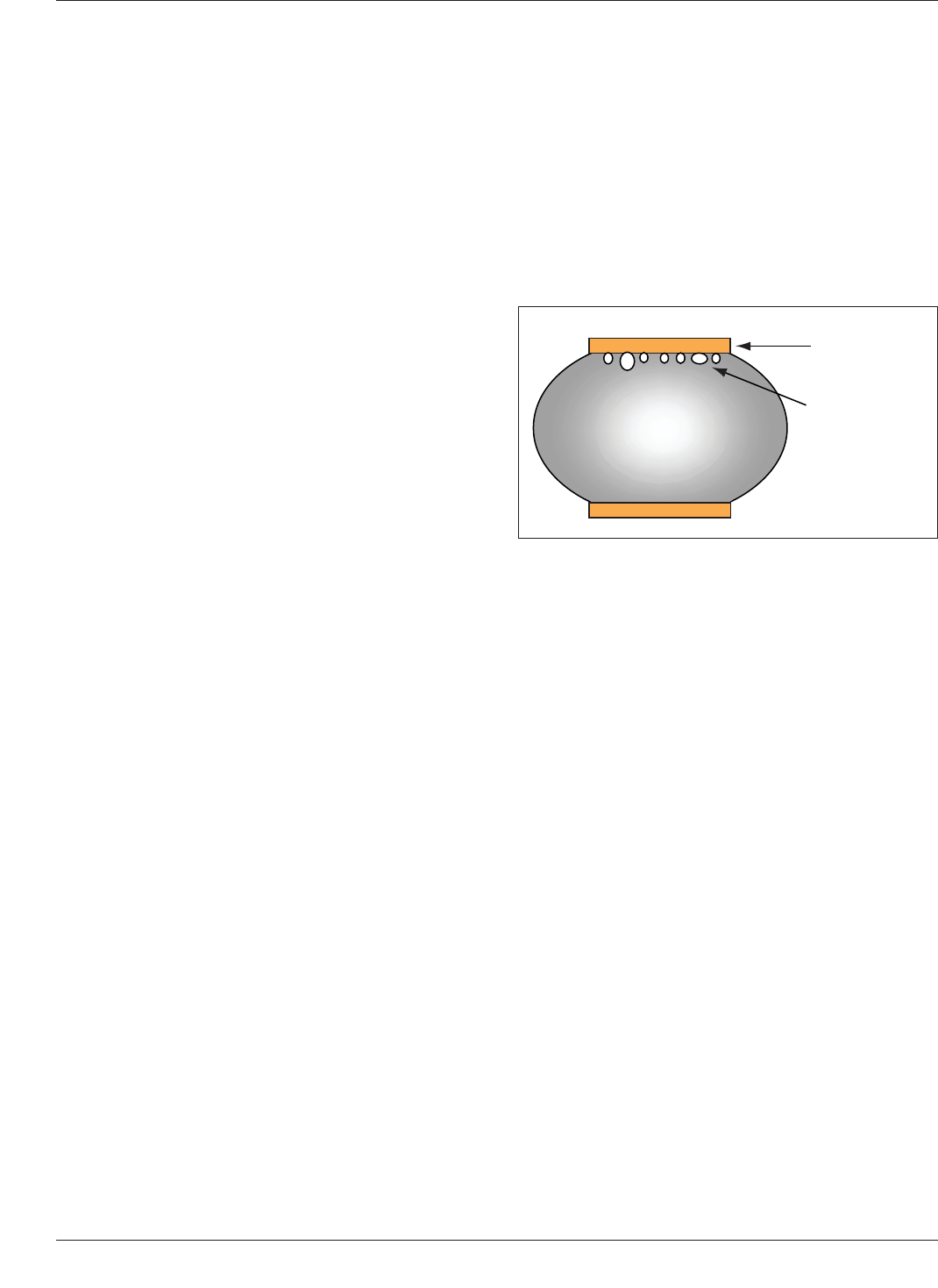
Voiding can be a result of surface contamination at the
component land or PCB land, intermetallics forming
between solder ball and land, or un-expelled flux residues
from the assembly process as shown in Figure 7-42.
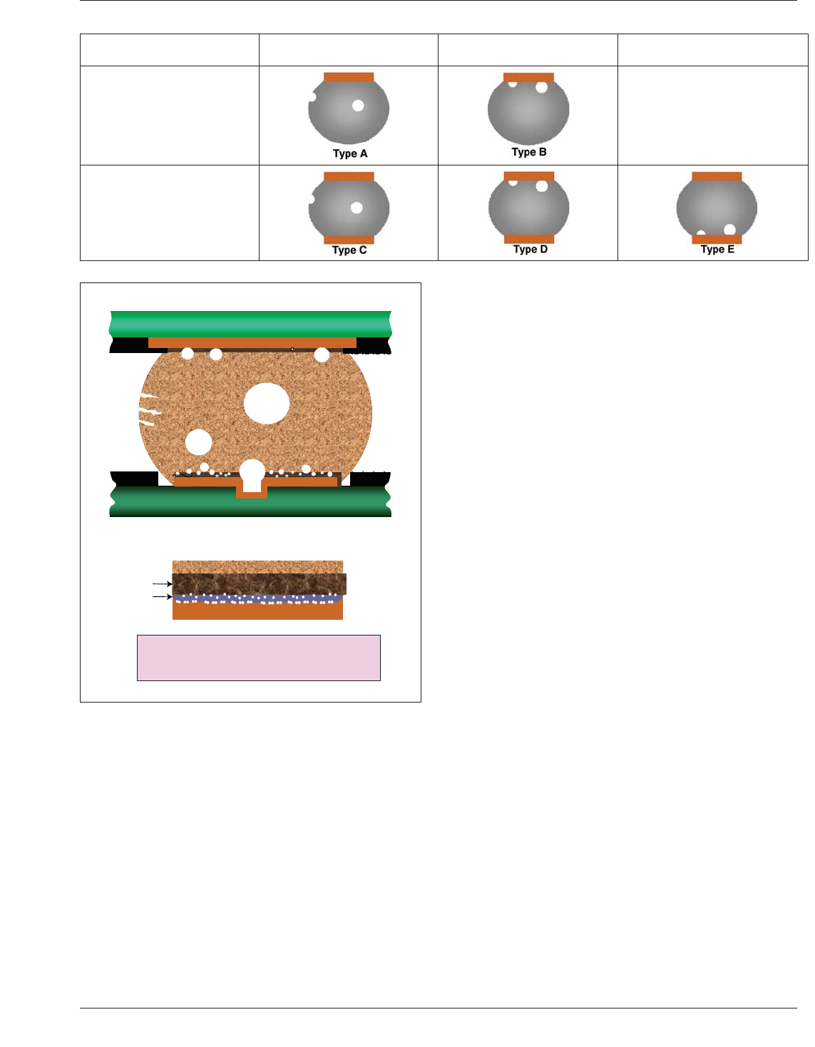
7.5.2 Void Classification In order to assess different
conditions, voids have been given a specific identifier,
based on location, to establish a method of void identifica-
tion and the possibility of corrective action for process
improvement. The details are provided in Table 7-6 which
shows classification criteria for the location of voids in the
BGA solder ball structure.
The following descriptions identify the five different void
types:
Type A: Void(s) within the ball (package level) as
received.
Type B: Void(s) at the ball/package substrate interface as
received.
Type C: Void(s) within the ball after board level assembly
process.
Type D: Void(s) at the ball/package substrate interface
after board level assembly process.
Type E: Void(s) at the ball/board substrate interface after
board level assembly process.
7.5.3 Voids in BGA Solder Joints Six types of voids in
solder joints have been identified and described. The char-
acteristics of each of these voids are summarized in Figure
7-43 which illustrates the typical size and location of these
voids in a BGA solder joint.
7.5.3.1 Macrovoids Macrovoids are the most widely
occurring voids in solder joints. These are caused by vola-
tile compounds that evolve during the soldering processes.
IPC-7095c-7-42
Figure 7-42 Small Voids Clustered in Mass at the Ball-to-
Land Interface
Land Pattern
on Package
Small Voids
at Ball-to-Land
Interface
IPC-7095C January 2013
102
Copyright IPC-Association Connecting Electronics Industries
Provided by IHS under license with IPC
Not for Resale
No reproduction or networking permitted without license from IHS
--`,,```,,,,````-`-`,,`,,`,`,,`---
These macrovoids generally do not affect the solder joint
reliability unless they are present at interfacial regions in
the solder joints where cracks typically propagate.
7.5.3.2 Planar Microvoids Planar Microvoids are a
series of small voids, in relatively the same plane, located
at the interface between the PCB Lands and the solder.
These are caused by copper caves under ImAg surface-
finish coated lands. They do not affect initial product qual-
ity, but can affect long term solder joint reliability. They
can be eliminated by strict control of the ImAg surface fin-
ish plating solutions and etching chemicals and other criti-
cal process parameters, at all times during surface finish
plating on boards.
7.5.3.3 Shrinkage Voids Shrinkage Voids are caused by
the shrinkage during solidification, mostly for SAC and
other lead-free solders. They do not generally appear near
the solder-to-PCB land interface and do not impair the
solder joint reliability. These shrinkage voids can be mini-
mized by increasing the cooling rate during soldering and
avoiding disturbance to the joint while it’s solidifying. Fun-
damentally these shrinkage voids are surface cracks and do
not pose any reliability problems.
7.5.3.4 Microvia Voids Microvia Voids are caused by the
presence of micro-vias designed in the PCB lands. Large
Micro-via Voids, if located in solder joints in high stress
areas of a package, can impact solder joint reliability. Plat-
ing the micro-via shut, or filling it completely with solder
paste by double printing, can minimize the creation of
these voids.
7.5.3.5 IMC Microvoids IMC Microvoids occur within
the Intermetallic Compound (IMC) formed between copper
and high tin solders, including SAC and tin/lead solders.
These IMC Microvoids do not form immediately after the
soldering process, but after aging at high temperatures or
during temperature cycling of the solder joints. The true
root cause is still under investigation, but a Kirkendall
voiding mechanism may play a part. These voids can affect
solder joint reliability, particularly in instances when brittle
fracture is initiated within the IMC during drop or
mechanical shock to the solder joint. Doping the solder
with certain elements such as zinc is one way to diminish
the amount of these IMC microvoids.
7.5.3.6 Pinhole Voids Pinhole Voids are caused by pin-
holes in the copper lands of the PCB. With sufficient quan-
tity, they can affect solder joint reliability. These voids are
caused by entrapped PCB fabrication chemicals within
these pinholes that volatilize during the reflow soldering
process. The pinholes occur due to an excursion within the
copper plating process at the PCB fabricator and can
be eliminated by improved copper plating process control
systems.
Table 7-6 Void Classification
Void Analysis Voids Within the Ball
Voidsatthe
Package Interface
Voids at the Mounting
Surface Interface
Voids in BGA balls prior to
attachment to a PWB
N/A
Voids in BGA balls after
attachment to a PWB
IPC-7095c-7-43
Figure 7-43 Typical Size and Location of Various Types of
Voids in a BGA Solder Joint
1
1
1
1
1
2
2
2
4
6
6
1
1
1
1
1
2
2
2
3
5
4
6
6
BGA Solder Joint after Reflow Soldering
Cu-IMC-Solder Interface
after High Temp Aging
Cu
6
Sn
5
Cu
6
Sn
1: Macrovoids
2: Planar Microvoids
3: Shrinkage Voids
4: Micro-Via Voids
5: IMC Microvoids
6: Pinhole Voids
January 2013 IPC-7095C
103
Copyright IPC-Association Connecting Electronics Industries
Provided by IHS under license with IPC
Not for Resale
No reproduction or networking permitted without license from IHS
--`,,```,,,,````-`-`,,`,,`,`,,`---