MDS-C1-SPA Series INSTRUCTION MANUALib1500152(eng)a.pdf - 第89页
3. Setup 3 - 29 (5) Confirming the Z phase pulse width Check the output signal waveform by measuring the signals of the che ck terminals on the PCB with the DC range of the synchroscope. A phase output signal ...... Acro…
3. Setup
3 - 28
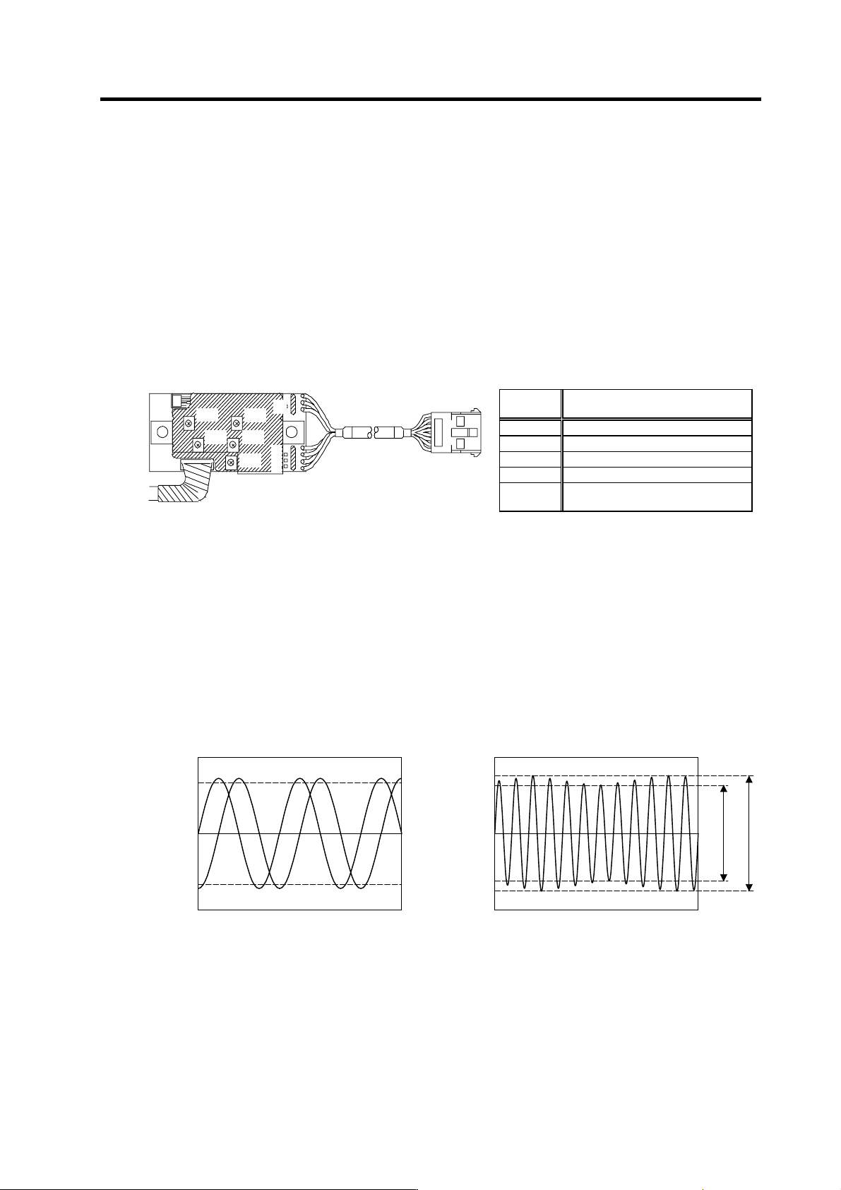
(4) Adjusting the A phase and B phase output signal
[1] Set the drive unit in the open loop operation state. (Set the spindle parameter SP038/bitF to
"1" and turn the spindle drive unit power ON again.) There are cases when sudden speed
changes cannot be followed during open loop operation, so gradually change the speed
command.
[2] Forward run the motor and rotate the PLG at the reference speed.
[3] Using the PCB volume VR1 to VR4, adjust so that the A phase and B phase signals are within
the specified range. If the correct waveform cannot be attained even after adjusting with VR1
to VR4, adjust the gap again.
[4] Reverse run the motor and rotate the PLG at the reference speed.
[5] Adjust the output waveform by adjusting VR1 to VR4 in the same manner.
VR1
VR2
VR4
VR3
VR5
G
B
A
Z
PCB section
[6] Set the spindle drive unit to the closed loop operation state (normal operation).
[7] Run the motor at the maximum speed, and confirm that the A phase and B phase output
voltage peak value is larger than 0.8V on both the plus side and minus side during both
forward run and reverse run.
[8] Run the motor at the reference speed, and confirm that the A phase and B phase output signal
envelope is 0.4V or less.
The envelope is calculated by the expression below.
(Envelope) = (Maximum amplitude α) - (Minimum amplitude β)
[9] If the envelope is larger than the designated value, the deflection of the detection gears' outer
diameter may be large, so check the deflection.
Example of A phase/B phase signal waveform
during forward run at maximum speed
Definition of envelope
V
olume function
Check
terminal
Signal name
VR1 A phase offset adjustment
VR2 A phase gain adjustment
VR3 B phase offset adjustment
VR4 B phase gain adjustment
VR5
Z phase pulse width adjustment
(Already adjusted before shipment)
A phase
B
p
hase
0.8
Voltage [V]
-0.8
0
Time
Voltage [V]
0
Time
Minimum am
p
litude:
β
Maximum amplitude: α
3. Setup
3 - 29
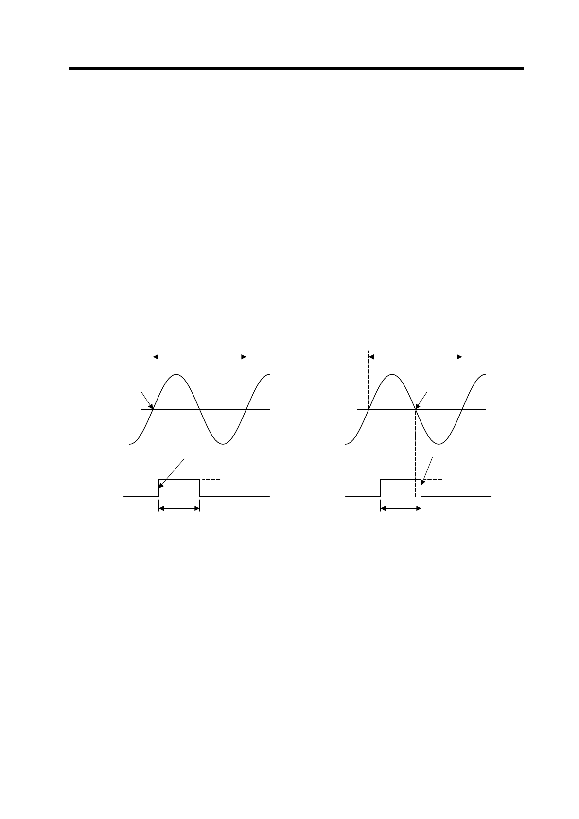
(5) Confirming the Z phase pulse width
Check the output signal waveform by measuring the signals of the check terminals on the PCB
with the DC range of the synchroscope.
A phase output signal...... Across A-G
Z phase output signal...... Across Z-G
The output signal waveform is confirmed during motor forward run and reverse run. Set the
synchroscope as follows to measure the waveform during each run direction.
During forward run .......... Apply a trigger at the rising edge of the Z phase output signal
During reverse run .......... Apply a trigger at the falling edge of the Z phase output signal
Confirm that the Z phase pulse width (time that the Z phase signal is at the "H" level = approx. 15V)
is 40% or more and 60% or less, when one cycle of the A phase signal is calculated as 100%. The
normal Z phase output signal waveform when run at the reference speed is shown below. If the
output signal waveform is not as shown below, refer to the next section "(6) Adjusting the Z phase
pulse width" and adjust.
The Z phase pulse width has been adjusted at shipment, with a combination of the sensor section
and PCB section having the same serial No. Thus, it normally does not need to be adjusted. If a
sensor section and PCB section having different serial numbers must be used, causing the Z
phase pulse width to deviate from the specified range, carry out the adjustment.
A phase/Z phas e output signal waveform
during forward run
A pha se/Z phas e output signal waveform
during reverse run
(6) Adjusting the Z phase pulse width
The Z phase pulse width can be adjusted with potentiometer VR5 on the PCB. VR5 is fixed after it
has been tested and adjusted to match the sensor section and PCB section having the same serial
No., so do not turn it unless a sensor section and PCB section with different serial numbers must
be used.
A phase
0V
One A
p
hase c
y
cle = 100%
R
p
oint
Z phase pulse width: 40 to 60%
A
pply a trigger at the falling
edge of the Z phase
H level (reference
volta
g
e +15V
)
L level
Z phase
A phase
0V
One A
p
hase c
y
cle = 100%
Q
p
oint
A
pply a trigger at the rising
edge of the Z phase
H level (reference
volta
g
e +15V
)
L level
Z
p
hase
Z phase pulse width: 40 to 60%
3. Setup
3 - 30
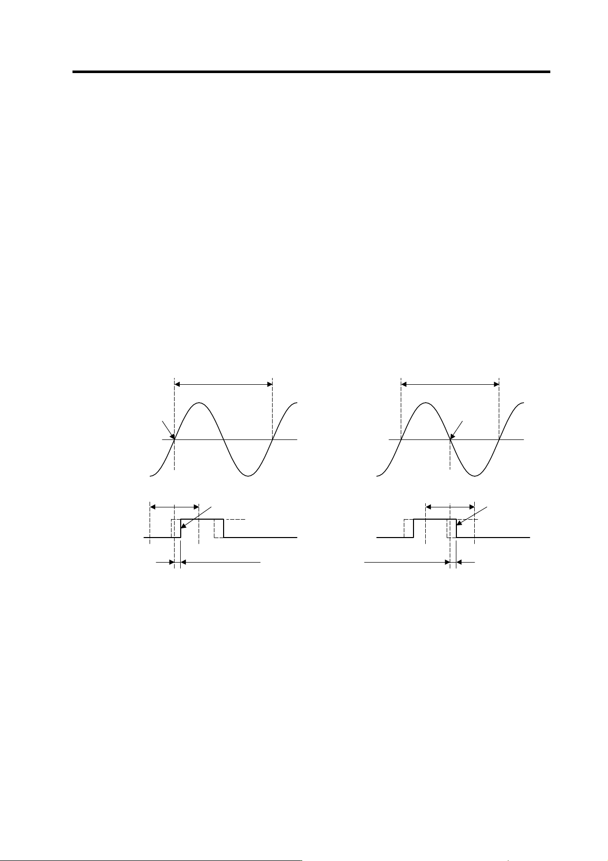
(7) Checking the Z phase and A phase difference
Check the output signal waveform by measuring the signals of the check terminals on the PCB
with the DC range of the synchroscope.
A phase output signal...... Across A-G
Z phase output signal...... Across Z-G
The output signal waveform is confirmed during motor forward run and reverse run. Set the
synchroscope as follows to measure the waveform during each run direction.
During forward run ..... Apply a trigger at the rising edge of the Z phase output signal
During reverse run ..... Apply a trigger at the falling edge of the Z phase output signal
The phase difference for the Z phase signal and A phase signal is defined as follows.
During forward run ..... Time difference between Z phase output signal rising edge and A
phase output signal zero point (Q point)
During reverse run ..... Time difference between Z phase output signal falling edge and A
phase output signal's 1/2 cycle point (R point)
Confirm that the phase difference between the Z phase to the A phase is within ±25% during both
forward and reverse run when one cycle of the A phase signal is calculated as100%. If the output
signal waveform is not as shown below, refer to the next section "(8) Adjusting the Z phase and A
phase difference" and adjust.
Confirming the Z phase signal phase difference
during forward run
Confirming the Z phase signal phase difference
during reverse run
One A
p
hase c
y
cle = 100%
One A
p
hase c
y
cle = 100%
Phase difference of
A
phase and Z phase
Tolerable
range of phase
difference
±
25%
Phase difference of A phase and Z phase
Tolerable
range of phase
difference
±
25%
A phase
0V
R
p
oint
A
pply a trigger at the falling
edge of the Z phase
H level (reference
volta
g
e +15V
)
L level
Z phase
A phase
0V
Q
p
oint
A
pply a trigger at the rising
edge of the Z phase
H level (reference
volta
g
e +15V
)
L level
Z
p
hase