743844-015.pdf - 第115页
Technology Form Factor Ball Count Processor LPDDR4x 1 x64 (1R, 2R) 1 432 P/U/U Refresh - Processor LPDDR4x 1 х64 (1R, 2R) 1 556 P/U/U Refresh - Processor LPDDR5/x 1 x64 (1R, 2R) 1 496 P/PX/U/U Refresh - Processor LPDDR5/…
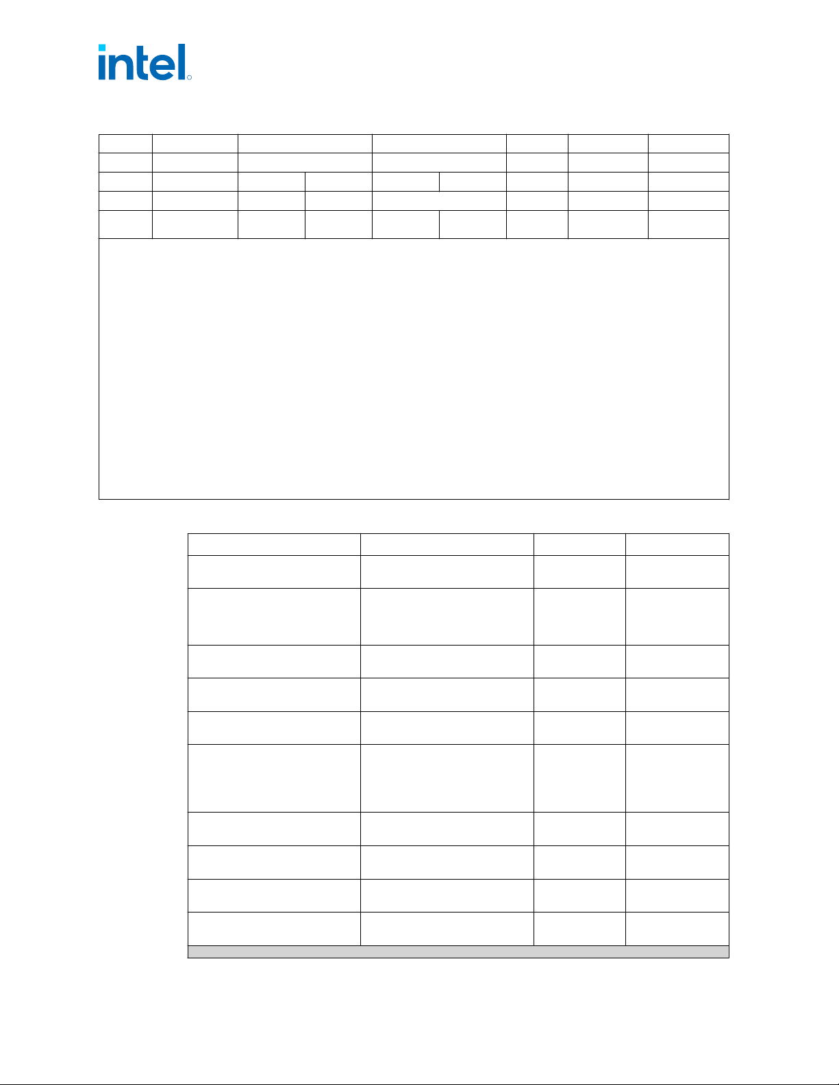
Processor Technology DDR4 DDR5
16
LPDDR4x LPDDR5
13
LPDDR5x
13
VDD2 [V]
5
1.2 1.1 1.1 1.05 1.05
Maximum RPC
2
2 4 2 4 2 2 2
Die Density [Gb] 8,16 8,16 16 , 24
15
8,16 8, 12 ,16 8, 12 ,16
Ballmap Mode
10
IL /NIL IL /NIL P : NIL, S LGA
- IL
NIL NIL
NIL NIL
Notes: 1. 1DPC refer to system with one DIMM slot routed per 64-bit channel, 2DPC refer to system with two DIMM slots routed per 64-bit channel.
2. RPC = Rank Per Channel.
3. Memory down of all technologies should be implemented homogeneous means that all DRAM devices should be from the same vendor and have the
same part number. Implementing a mix of DRAM devices may cause serious signal integrity and functional issues.
4. There is no support for memory modules with different technologies or capacities on opposite sides of the same memory module. If one side of a
memory module is populated, the other side is either identical or empty.
5. VDD2 is Processor DRAM voltage; VDDQ is DRAM voltage.
6. DDR5 2R 5600 is pending Intel enablement.
7. Maximum 2DPC frequency supported when same DIMM part number populated Within channel. Frequency is not guaranteed when mix DIMM's
populated..
8. DDR5 5V is SODIMM/UDIMM voltage, 1.1V is Memory down voltage.
9. DDR4/DDR5 SoDIMM 2DPC Is not for S/S Refresh/E/E Refresh -Processor Line.
10. L/NIL mode depends on Memory topology
11. Far memory slot to be populated, in case, single DIMM is placed on 2DPC channel.
12. DDR4/DDR5 ECC is supported only when all populated memory modules in system are support ECC, ECC supported by specific S/S Refresh/E-
Processor Line HX/HX Refresh SKUs.
13. LPDDR5 technology supports 8 Bank Mode, BG (Bank Group) Mode and 16 Bank Mode.LPDDR5x technology supports BG Mode and 16 Bank Mode,
according to JEDEC spec.
The Processor supports BG Mode and 16 Bank Mode. Bank Mode may vary according to SAGV Point.
14. LPDDR5 2R 6400MT/s is pending Intel enablement.
15. DDR5 24Gb die density is POR post TTM.
16. S/S Refresh-DDR5 8+8/6+0 DDR5 speed follows Gen 12 DDR5 speeds. HX 8+8 DDR5 speed follows Gen12 8+8 DDR5 speeds
17. DDR POR speed refers to Processor top SKU. Other SKUs may use lower memory speed, please refer to ark.intel.com for top memory speed.
Table 26. DDR Technology Support Matrix
Technology Form Factor Ball Count Processor
DDR4 UDIMM 288 S/S Refresh-
Processor
DDR4 SoDIMM 260
S/H/HX/P/U/U
Refresh/HX
Refresh -
Processor
DDR4
1
x16 SDP (1R)
1
96
H/P/U/U Refresh -
Processor
DDR4
1
x16 DDP (1R)
1
96
H/P/U/U Refresh -
Processor
DDR4
1
x8 SDP (1R)
1
78
H/P/U/U Refresh -
Processor
DDR5 SoDIMM 262 H/HX/P/U/S/S
Refresh/U
Refresh/HX
Refresh/U Refresh
- Processor
DDR5 UDIMM 288
S/S Refresh/E/E
Refresh -Processor
DDR5
1
x8 SDP (1R)
1
78
H/P/U/U Refresh -
Processor
DDR5
1
x16 SDP (1R)
1
102
H/P/U/U Refresh -
Processor
LPDDR4x
1
x32 (1R, 2R)
1
200
H/P/U/U Refresh -
Processor
continued...
R
Intel
®
Core
™
, Xeon
™
6300 And Xeon
™
E 2400 Processors—Memory
13
th
Generation Intel
®
Core
™
, Intel
®
Core
™
14
th
Generation, Intel
®
Core
™
Processor (Series 1) and (Series 2), Intel
®
Xeon
™
E
2400 Processor and Intel
®
Xeon
™
6300 Processor
Datasheet, Volume 1 of 2 May 2025
114 Doc. No.: 743844, Rev.: 015
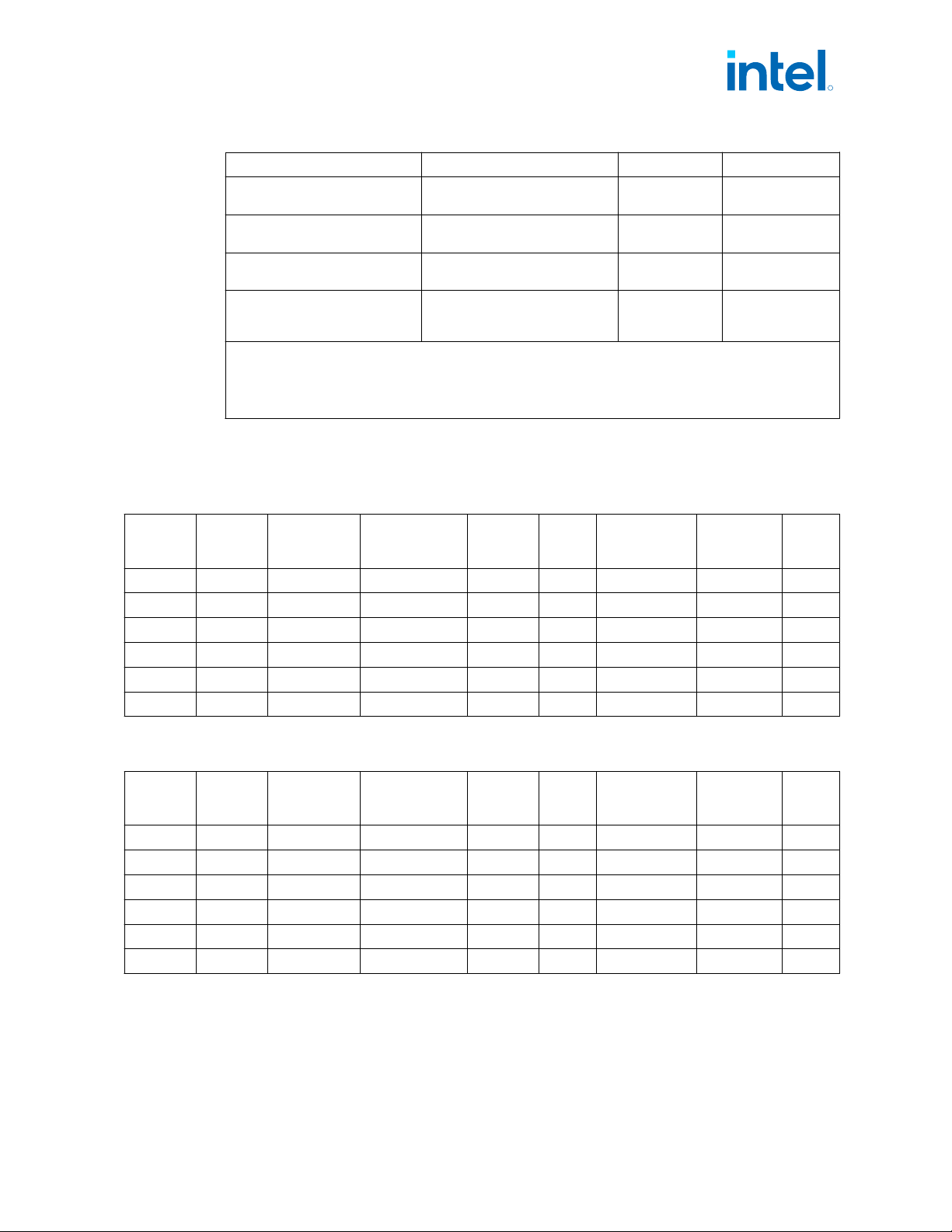
Technology Form Factor Ball Count Processor
LPDDR4x
1
x64 (1R, 2R)
1
432
P/U/U Refresh -
Processor
LPDDR4x
1
х64 (1R, 2R)
1
556
P/U/U Refresh -
Processor
LPDDR5/x
1
x64 (1R, 2R)
1
496
P/PX/U/U Refresh
- Processor
LPDDR5/x
1
x32 (1R, 2R)
1
315
H/P/PX/U/U
Refresh -
Processor
Note: 1. Memory down of all technologies should be implemented homogeneously, which means that all
DRAM devices should be from the same vendor and have the same part number. Implementing
a mix of DRAM devices may cause serious signal integrity and functional issues, DDR4/DDR5
restriction is for single MC configuration, LPDDR4x/LPDDR5/x restriction is for both MC
configuration (all DRAMs in the system must be from same Part Number).
Supported Memory Modules and Devices
Table 27. Supported DDR4 Non-ECC SoDIMM Module Configurations (S/S
Refresh/H/HX/P/U/HX Refresh/U Refresh - Processor Line)
Raw
Card
Version
DIMM
Capacity
DRAM
Device
Technology
DRAM
Organization
# of
DRAM
Devices
# of
Ranks
# of Row/Col
Address Bits
# of Banks
Inside
DRAM
Page
Size
A 8 GB 8 Gb 1024M x 8 8 1 16/10 16 8K
A 16 GB 16 Gb 2048M x 8 8 1 17/10 16 8K
C 4 GB 8 Gb 512M x 16 4 1 16/10 8 8K
C 8 GB 16 Gb 1024M x 16 4 1 17/10 8 8K
E 16 GB 8 Gb 1024M x 8 16 2 16/10 16 8K
E 32 GB 16 Gb 2048M x 8 16 2 17/10 16 8K
Table 28. Supported DDR4 ECC SoDIMM Module Configurations (S/S Refresh/HX/HX
Refresh - Processor Line)
Raw
Card
Version
DIMM
Capacity
DRAM
Device
Technology
DRAM
Organization
# of
DRAM
Devices
# of
Ranks
# of Row/Col
Address Bits
# of Banks
Inside
DRAM
Page
Size
D 8 GB 8 Gb 1024M x 8 9 1 16/10 16 8K
D 16 GB 16 Gb 2048M x 8 9 1 17/10 16 8K
G 16 GB 8 Gb 1024M x 8 18 2 16/10 16 8K
G 32 GB 16 Gb 2048M x 8 18 2 17/10 16 8K
F 16 GB 8 Gb 1024M x 8 18 2 16/10 16 8K
F 32 GB 16 Gb 2048M x 8 18 2 17/10 16 8K
5.1.2
R
Memory—Intel
®
Core
™
, Xeon
™
6300 And Xeon
™
E 2400 Processors
13
th
Generation Intel
®
Core
™
, Intel
®
Core
™
14
th
Generation, Intel
®
Core
™
Processor (Series 1) and (Series 2), Intel
®
Xeon
™
E
2400 Processor and Intel
®
Xeon
™
6300 Processor
May 2025 Datasheet, Volume 1 of 2
Doc. No.: 743844, Rev.: 015 115
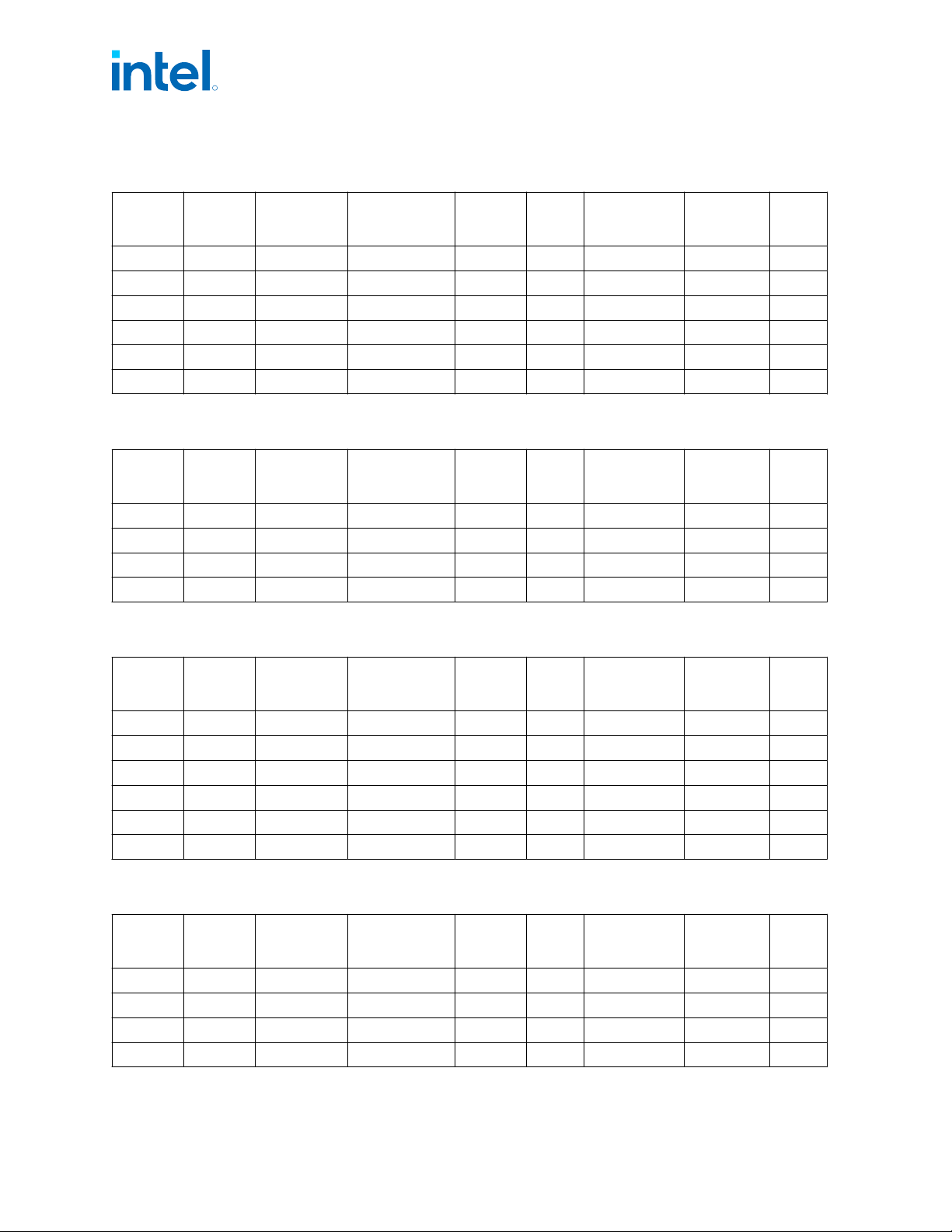
Table 29. Supported DDR4 Non-ECC UDIMM Module Configurations (S/S Refresh -
Processor Line)
Raw
Card
Version
DIMM
Capacity
DRAM
Device
Technology
DRAM
Organization
# of
DRAM
Devices
# of
Ranks
# of Row/Col
Address Bits
# of Banks
Inside
DRAM
Page
Size
A 8 GB 8 Gb 1024M x 8 8 1 16/10 16 8K
A 16 GB 16 Gb 2048M x 8 8 1 17/10 16 8K
C 4 GB 8 Gb 512M x 16 4 1 16/10 8 8K
C 8 GB 16 Gb 1024M x 16 4 1 17/10 8 8K
B 16 GB 8 Gb 1024M x 8 16 2 16/10 16 8K
B 32 GB 16 Gb 2048M x 8 16 2 17/10 16 8K
Table 30. Supported DDR4 ECC UDIMM Module Configurations (S/S Refresh - Processor
Line)
Raw
Card
Version
DIMM
Capacity
DRAM
Device
Technology
DRAM
Organization
# of
DRAM
Devices
# of
Ranks
# of Row/Col
Address Bits
# of Banks
Inside
DRAM
Page
Size
D 8 GB 8 Gb 1024M x 8 9 1 16/10 16 8K
D 16 GB 16 Gb 2048M x 8 9 1 17/10 16 8K
E 16 GB 8 Gb 1024M x 8 18 2 16/10 16 8K
E 32 GB 16 Gb 2048M x 8 18 2 17/10 16 8K
Table 31. Supported DDR5 Non-ECC SoDIMM Module Configurations (S/S Refresh/H/H
Refresh/HX/P/U/HX Refresh/U Refresh - Processor Line)
Raw
Card
Version
DIMM
Capacity
DRAM
Device
Technology
DRAM
Organization
# of
DRAM
Devices
# of
Ranks
# of Row/Col
Address Bits
# of Banks
Inside
DRAM
Page
Size
A 16 GB 16 Gb 2048M x 8 8 1 17/10 16 8K
C 8 GB 16 Gb 1024M x 16 4 1 17/10 8 8K
B 32 GB 16 Gb 2048M x 8 16 2 17/10 16 8K
A 24 GB 24 Gb 3072M x 8 8 1 17/10 32 8K
C 12 GB 24 Gb 1536M x 16 4 1 17/10 16 8K
B 48 GB 24 Gb 3072M x 8 16 2 17/10 32 8K
Table 32. Supported DDR5 ECC SoDIMM Module Configurations (S/S Refresh/HX/HX
Refresh - Processor Line)
Raw
Card
Version
DIMM
Capacity
DRAM
Device
Technology
DRAM
Organization
# of
DRAM
Devices
# of
Ranks
# of Row/Col
Address Bits
# of Banks
Inside
DRAM
Page
Size
D 16 GB 16 Gb 2048M x 8 9 1 17/10 16 8K
E 32 GB 16 Gb 2048M x 8 18 2 17/10 16 8K
D 24 GB 24 Gb 3072M x 8 9 1 17/10 32 8K
E 48 GB 24 Gb 3072M x 8 18 2 17/10 32 8K
R
Intel
®
Core
™
, Xeon
™
6300 And Xeon
™
E 2400 Processors—Memory
13
th
Generation Intel
®
Core
™
, Intel
®
Core
™
14
th
Generation, Intel
®
Core
™
Processor (Series 1) and (Series 2), Intel
®
Xeon
™
E
2400 Processor and Intel
®
Xeon
™
6300 Processor
Datasheet, Volume 1 of 2 May 2025
116 Doc. No.: 743844, Rev.: 015