743844-015.pdf - 第120页
System Memory Timing Support Table 41. DDR System Memory Timing Support DRAM Device Transfer Rate (MT/s) tCL (tCK) tRCD (ns) tRP (ns) CWL (tCK) DPC CMD Mode DDR4 3200 22 13.75 13.75 9-12, 14,16,18,20 1,2 2N DDR5 4000 36 …
Table 39. Supported LPDDR5/x x32 DRAMs Configurations (H/P/PX/U/U Refresh -
Processor Line)
Maximum System
Capacity
3
PKG
Type
(Die bits per Ch x PKG bits)
2
Die Density PKG Density Rank Per PKGs
12 GB
4
DDP 16x32 12 Gb 24 Gb 1
24 GB
4
QDP 16x32 12 Gb 48 Gb 2
16 GB DDP 16x32 16 Gb 32 Gb 1
32 GB QDP 16x32 16 Gb 64 Gb 2
64 GB
4
ODP 16x32 16 Gb 128 Gb 2
8 GB DDP 16x32 8 Gb 16 Gb 1
16 GB QDP 16x32 8 Gb 32 Gb 2
32 GB ODP 16x32 8 Gb 64 Gb 2
Notes: 1. x32 BGA devices are 315 balls
2. QDP - Quad Die Package, ODP - Octal Die Package, DDP - Dual Die Package
3. Maximum system capacity refers to system with all 8 sub-channels populated
4. Pending DRAM samples availability.
Table 40. Supported LPDDR5/x x64 DRAMs Configurations (P/PX/U/U Refresh -
Processor Line)
Maximum System
Capacity
2
PKG
Type
(Die bits per Ch x PKG
bits)
Die Density PKG Density Rank Per PKGs
16 GB QDP 16x64 16 Gb 64 Gb 1
32 GB ODP 16x64 16 Gb 128 Gb 2
8 GB QDP 16x64 8 Gb 32 Gb 1
16 GB ODP 16x64 8 Gb 64 Gb 2
Notes: 1. QDP - Quad Die Package, ODP - Octal Die Package
2. Maximum system capacity refers to system with all 8 sub-channels populated
System Memory Timing Support
The IMC supports the following DDR Speed Bin, CAS Write Latency (CWL), and
command signal mode timings on the main memory interface:
• tCL = CAS Latency
• tRCD = Activate Command to READ or WRITE Command delay
• tRP = PRECHARGE Command Period
• tRPb = per-bank PRECHARGE time
• tRPab = all-bank PRECHARGE time
• CWL = CAS Write Latency
• Command Signal modes:
— 2N indicates a new DDR5/DDR4/LPDDR4x/LPDDR5/x command may be issued
every 2 clocks
— 1N indicates a new DDR5/DDR4/LPDDR4x/LPDDR5/x command may be issued
every clock.
5.1.3
R
Memory—Intel
®
Core
™
, Xeon
™
6300 And Xeon
™
E 2400 Processors
13
th
Generation Intel
®
Core
™
, Intel
®
Core
™
14
th
Generation, Intel
®
Core
™
Processor (Series 1) and (Series 2), Intel
®
Xeon
™
E
2400 Processor and Intel
®
Xeon
™
6300 Processor
May 2025 Datasheet, Volume 1 of 2
Doc. No.: 743844, Rev.: 015 119
System Memory Timing Support
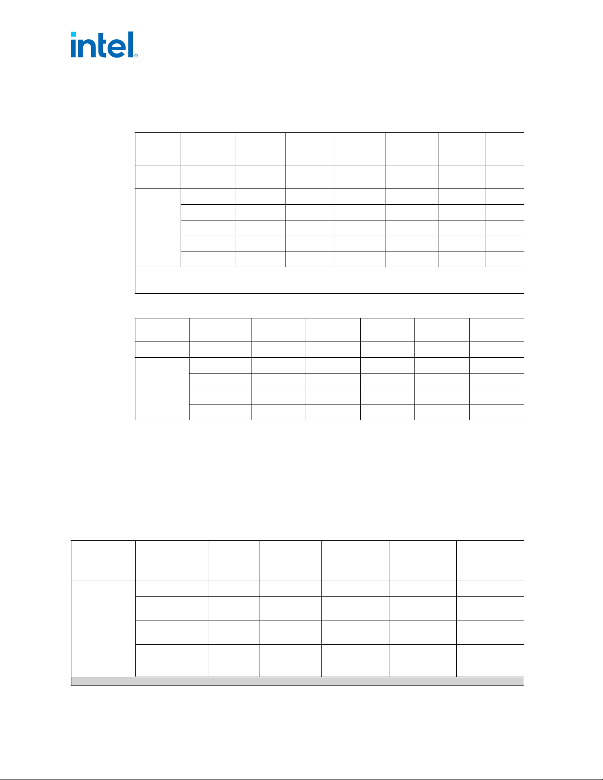
Table 41. DDR System Memory Timing Support
DRAM
Device
Transfer
Rate
(MT/s)
tCL (tCK) tRCD (ns) tRP (ns) CWL (tCK) DPC
CMD
Mode
DDR4 3200 22 13.75 13.75
9-12,
14,16,18,20
1,2 2N
DDR5
4000 36 17 17.00 34 1 2N
4400 40 16.82 16.82 38 1,2
1
2N
4800 42 16.67 16.67 40 1 2N
5200 46 16.153 16.153 44 1 2N
5600 50 16.42 16.42 48 1 2N
Note:
1. 2 DPC supported when one slot is populated in each channel
Table 42. LPDDR System Memory Timing Support
DRAM
Device
Transfer Rate
(MT/s)
tCL (tCK) tRCD (ns) tRPpb (ns) tRPab (ns)
WL (tCK)
Set B
LPDDR4x 4266 36 18 18 21 34
LPDDR5/x
4800 13 18.33 18.33 21.67 12
5200 15 18.46 18.46 21.54 14
6000 16 18.72 18.46 21.28 15
6400 17 18.75 18.75 21.25 16
SAGV Points
SAGV (System Agent Geyserville) is a way by which they SoC can dynamically scale
the work point (V/F), by applying DVFS (Dynamic Voltage Frequency Scaling) based
on memory bandwidth utilization and/or the latency requirement of the various
workloads for better energy efficiency at System-Agent.heuristics are in charge of
providing request for work points by periodically evaluating the utilization of the
memory and IA stalls.
Table 43. SA Speed Enhanced Speed Steps (SA-GV) and Gear Mode Frequencies
Processor Technology
DDR
Maximum
Rate
[MT/s]
SAGV-LowBW SAGV-MedBW SAGV-HighBW
SAGV-
MaxBW/
lowest latency
Processor
4,5
S/S refresh/HX
DDR4 3200 2133 G2 2666 G1 2933 G1 3200 G1
DDR5 1DPC 2R
UDIMM / SODIMM
5200 2000 G2 3600 G2 4800 G2 5200 G2
DDR5 1DPC 1R
UDIMM /SODIMM
5600 2000 G2 3600 G2 5200 G2 5600 G2
DDR5 1DPC 2R
UDIMM S-Refresh
only
7
5600 2000 G2 3600 G2 5200 G2 5600 G2
continued...
5.1.3.1
5.1.3.2
R
Intel
®
Core
™
, Xeon
™
6300 And Xeon
™
E 2400 Processors—Memory
13
th
Generation Intel
®
Core
™
, Intel
®
Core
™
14
th
Generation, Intel
®
Core
™
Processor (Series 1) and (Series 2), Intel
®
Xeon
™
E
2400 Processor and Intel
®
Xeon
™
6300 Processor
Datasheet, Volume 1 of 2 May 2025
120 Doc. No.: 743844, Rev.: 015
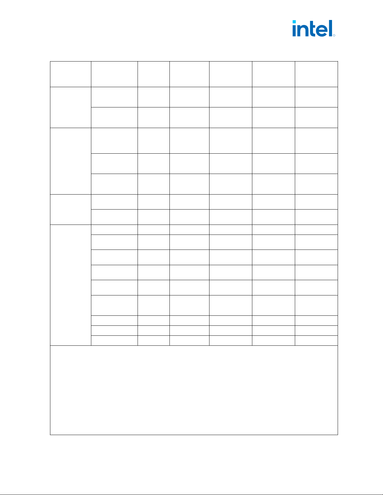
Processor Technology
DDR
Maximum
Rate
[MT/s]
SAGV-LowBW SAGV-MedBW SAGV-HighBW
SAGV-
MaxBW/
lowest latency
DDR5 1DPC on
2DPC UDIMM S
only
4400 2000 G2 3600 G2 4000 G2 4400 G2
DDR5 1DPC on
2DPC SODIMM
(HX only)
4000 2000 G2 3600 G2 3600 G2 4000 G2
Processor
4,5
HX
Refresh
DDR5 1DPC on
2DPC 1R
SODIMMHX
Refresh only
7
4400 2000 G2 3600 G2 4000 G2 4400 G2
DDR5
6,7
2DPC
1R/1R HX Refresh
only
4400 2000 G2 3600 G2 4000 G2 4400 G2
DDR5
6,7
2DPC
2R/2R HX Refresh
only
4000 2000 G2 3600 G2 3600 G2 4000 G2
Processor
4,5
S/S refresh/HX
DDR5
6
2DPC
1R/1R
4000 2000 G2 3600 G2 3600 G2 4000 G2
DDR5
6
2DPC
2R/2R
3600 2000 G2 3200 G2 3200 G2 3600 G2
Processor
5
H/P/U/U-
Refresh /H-
Refresh
LPDDR4x 4266 2666 G4 3733 G4 4266G4 4266 G2
LPDDR5/x 1R PCB
T4
6400 2400 G4 6000 G4 6400 G4 5200 G2
LPDDR5/x 2R PCB
T4 Refresh only
7
6400 2400 G4 6000 G4 6400 G4 5200 G2
LPDDR5/x 2R PCB
T4
6000 2400 G4 5600 G4 6000 G4 5200 G2
LPDDR5 2R PCB
T3
4800 2400 G4 4400 G4 4800 G4 4800 G2
LPDDR5 1R PCB
T3 LPDDR5x
1R/2R PCB T3
5200 2400 G4 4400 G4 5200 G4 4800 G2
DDR4 3200 2133 G2 2933 G2 3200 G2 2666 G1
DDR5 5600 2000 G2 3600 G2 5200 G2 5600 G2
DDR5 5200 2000 G2 3600 G2 4800 G2 5200 G2
Notes: 1. The Processor supports dynamic gearing technology where the Memory Controller can run at 1:1 (Gear-1,
Legacy mode) or 1:2 (Gear-2 mode) and 1:4 (Gear-4 mode) ratio of DRAM speed. The gear ratio is the ratio of
DRAM speed to Memory Controller Clock.
MC Channel Width equal to DDR Channel width multiply by Gear Ratio
2. SA-GV modes
a. LowBW- Low frequency point, Minimum Power point. Characterized by low power, low BW, high latency. The
system will stay at this point during low to moderate BW consumption.
b. MedBW - Tuned for balance between power & performance.
c. HighBW Characterized by high power, low latency, moderate BW also used as RFI mitigation point.
d. MaxBW/ lowest latency Lowest Latency point, low BW and highest power.
3. Intel
®
System Agent Enhanced Speed Step
®
is not enabled for S/S Refresh-Processor 125W/150W SKUs
4. SAGV point may change based on memory module Type.
5. On mixed module type configurations, the selected SAGV point will be the set to the lower frequency
configuration.
R
Memory—Intel
®
Core
™
, Xeon
™
6300 And Xeon
™
E 2400 Processors
13
th
Generation Intel
®
Core
™
, Intel
®
Core
™
14
th
Generation, Intel
®
Core
™
Processor (Series 1) and (Series 2), Intel
®
Xeon
™
E
2400 Processor and Intel
®
Xeon
™
6300 Processor
May 2025 Datasheet, Volume 1 of 2
Doc. No.: 743844, Rev.: 015 121