743844-015.pdf - 第210页
Symbol Parameter Minimum Typical Maximum Units Notes 1 R ON_DN(CK) Clock Buffer pull-down Resistance 30 — 45 Ω 5, 12 R ON_UP(CMD) Command Buffer pull-up Resistance 30 — 45 Ω 5, 12 R ON_DN(CMD) Command Buffer pull-down Re…
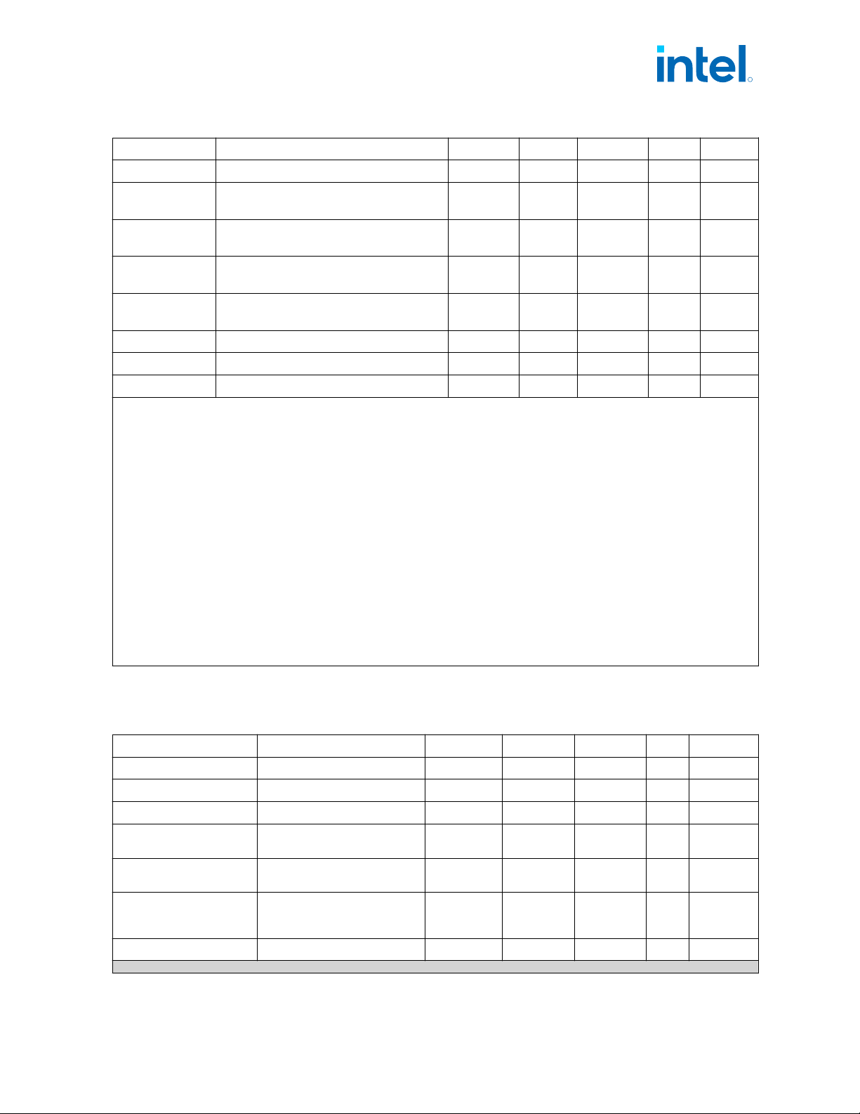
Symbol Parameter Minimum Typical Maximum Units Notes
1
R
ON_DN(CTL)
Control Buffer pull-down Resistance 30 50 Ω 5, 12
R
ON_UP
(SM_PG_CNTL1)
System Memory Power Gate Control Buffer
Pull-up Resistance
Ω —
R
ON_DN
(SM_PG_CNTL1)
System Memory Power Gate Control Buffer
Pull- down Resistance
Ω —
I
LI
Input Leakage Current (DQ, CK)
0 V , 0.2* VDD2, 0.8* VDD2
0.2 mA —
DDR0_VREF_DQ
DDR1_VREF_DQ
VREF output voltage
NA NA NA V —
SM_RCOMP[0] Command COMP Resistance 99 100 101 Ω 8
SM_RCOMP[1] Data COMP Resistance 99 100 101 Ω 8
SM_RCOMP[2] ODT COMP Resistance 99 100 101 Ω 8
Notes: 1. All specifications in this table apply to all processor frequencies.Timing specifications only depend on the
operating frequency of the memory channel and not the maximum rated frequency
2. V
IL
is defined as the maximum voltage level at a receiving agent that will be interpreted as a logical low value.
3. V
IH
is defined as the minimum voltage level at a receiving agent that will be interpreted as a logical high value.
4. V
IH
and V
OH
may experience excursions above V
DD2
. However, input signal drivers should comply with the signal
quality specifications.
5. Pull up/down resistance after compensation (assuming ±5% COMP inaccuracy). Note that BIOS power training
may change these values significantly based on margin/power trade-off. Refer to processor I/O Buffer Models
for I/V characteristics.
6. ODT values after COMP (assuming ±5% inaccuracy). BIOS MRC can reduce ODT strength towards
7. The minimum and maximum values for these signals are programmable by BIOS to one of the two sets.
8. SM_RCOMP[x] resistance should be provided on the system board with 1% resistors. SM_RCOMP[x] resistors
are to VSS. Values are pre-silicon estimations and are subject to change.
9. SM_DRAMPWROK must have a maximum of 15 ns rise or fall time over VDD2 * 0.30 ±100 mV and the edge
must be monotonic.
10.SM_VREF is defined as V
DD2
/2 for DDR5
11.RON tolerance is preliminary and might be subject to change.
12.Maximum-minimum range is correct but center point is subject to change during MRC boot training.
13.Processor may be damaged if V
IH
exceeds the maximum voltage for extended periods.
LPDDR4x DC Specification
Table 88. LPDDR4x Signal Group DC Specifications
Symbol Parameter Minimum Typical Maximum Units Notes
1
V
IL
Input Low Voltage — 0.2*Vdd2 0.08*Vdd2 V 2, 3, 4
V
IH
0 = Input High Voltage 0.35*Vdd2 0.2*Vdd2 — V 2, 3, 4
R
ON_UP(DQ)
Data Buffer pull-up Resistance 30 — 50 Ω 5,12
R
ON_DN(DQ)
Data Buffer pull-down
Resistance
30 — 50 Ω 5,12
R
ODT(DQ)
On-die termination equivalent
resistance for data signals
40 — 200 Ω 6, 12
V
ODT(DC)
On-die termination DC working
point (driver set to receive
mode)
0.1*Vdd2 — 0.3*Vdd2 V 10
R
ON_UP(CK)
Clock Buffer pull-up Resistance 30 — 45 Ω 5, 12
continued...
13.2.2.3
R
Electrical Specifications—Intel
®
Core
™
, Xeon
™
6300 And Xeon
™
E 2400 Processors
13
th
Generation Intel
®
Core
™
, Intel
®
Core
™
14
th
Generation, Intel
®
Core
™
Processor (Series 1) and (Series 2), Intel
®
Xeon
™
E
2400 Processor and Intel
®
Xeon
™
6300 Processor
May 2025 Datasheet, Volume 1 of 2
Doc. No.: 743844, Rev.: 015 209
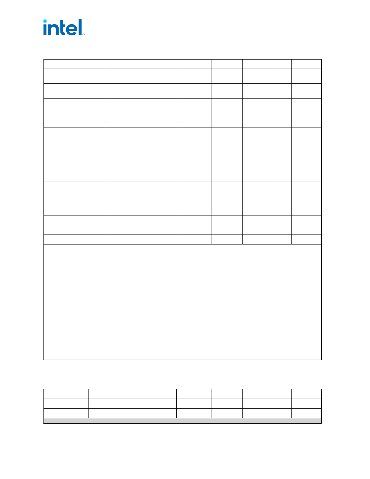
Symbol Parameter Minimum Typical Maximum Units Notes
1
R
ON_DN(CK)
Clock Buffer pull-down
Resistance
30 — 45 Ω 5, 12
R
ON_UP(CMD)
Command Buffer pull-up
Resistance
30 — 45 Ω 5, 12
R
ON_DN(CMD)
Command Buffer pull-down
Resistance
30 — 45 Ω 5, 12
R
ON_UP(CTL)
Control Buffer pull-up
Resistance
30 — 45 Ω 5, 12
R
ON_DN(CTL)
Control Buffer pull-down
Resistance
30 — 45 Ω 5, 12
R
ON_UP
(SM_PG_CNTL1)
System Memory Power Gate
Control Buffer Pull-up
Resistance
N/A — N/A Ω N/A
R
ON_DN
(SM_PG_CNTL1)
System Memory Power Gate
Control Buffer Pull- down
Resistance
N/A — N/A Ω N/A
I
LI
Input Leakage Current (DQ,
CK)
0 V
0.2* V
DD2
0.8* V
DD2
— — 1.1 mA —
SM_RCOMP[0] Command COMP Resistance 99 100 101 Ω 8
SM_RCOMP[1] Data COMP Resistance 99 100 101 Ω 8
SM_RCOMP[2] ODT COMP Resistance 99 100 101 Ω 8
Notes: 1. Unless otherwise noted, all specifications in this table apply to all processor frequencies. Timing specifications
only depend on the operating frequency of the memory channel and not the maximum rated frequency
2. V
IL
is defined as the maximum voltage level at a receiving agent that will be interpreted as a logical low value.
3. V
IH
is defined as the minimum voltage level at a receiving agent that will be interpreted as a logical high value.
4. V
IH
and V
OH
may experience excursions above V
DD2
. However, input signal drivers should comply with the signal
quality specifications.
5. Pull up/down resistance after compensation (assuming ±5% COMP inaccuracy). Note that BIOS power training
may change these values significantly based on margin/power trade-off. Refer to processor I/O Buffer Models
for I/V characteristics.
6. ODT values after COMP (assuming ±5% inaccuracy). BIOS MRC can reduce ODT strength towards
7. The minimum and maximum values for these signals are programmable by BIOS to one of the two sets.
8. SM_RCOMP[x] resistance should be provided on the system board with 1% resistors. SM_RCOMP[x] resistors
are to VSS. Values are pre-silicon estimations and are subject to change.
9. SM_DRAMPWROK must have a maximum of 15 ns rise or fall time over VDD2 * 0.30 ±100 mV and the edge
must be monotonic.
10.SM_VREF is defined as V
DD2
/2 for LPDDR4x
11.R
ON
tolerance is preliminary and might be subject to change.
12.Maximum-minimum range is correct but center point is subject to change during MRC boot training.
13.Processor may be damaged if V
IH
exceeds the maximum voltage for extended periods.
LPDDR5/x DC Specification
Table 89. LPDDR5/x Signal Group DC Specifications
Symbol Parameter Minimum Typical Maximum Units Notes
1
V
IL
Input Low Voltage - 0.15*Vdd2 0.06*Vdd2 V 2, 3, 4
V
IH
Input High Voltage 0.24*Vdd2 0.15*Vdd2 - V 2, 3, 4
continued...
13.2.2.4
R
Intel
®
Core
™
, Xeon
™
6300 And Xeon
™
E 2400 Processors—Electrical Specifications
13
th
Generation Intel
®
Core
™
, Intel
®
Core
™
14
th
Generation, Intel
®
Core
™
Processor (Series 1) and (Series 2), Intel
®
Xeon
™
E
2400 Processor and Intel
®
Xeon
™
6300 Processor
Datasheet, Volume 1 of 2 May 2025
210 Doc. No.: 743844, Rev.: 015
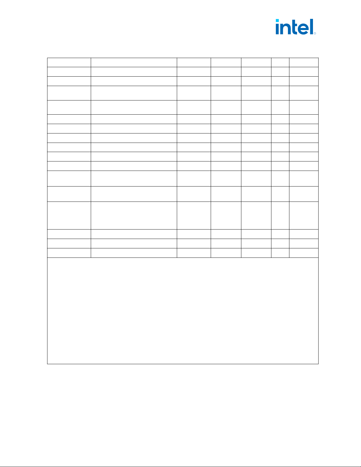
Symbol Parameter Minimum Typical Maximum Units Notes
1
R
ON_UP(DQ)
Data Buffer pull-up Resistance 30 50 Ω 5,12
R
ON_DN(DQ)
Data Buffer pull-down Resistance 30 50
R
ODT(DQ)
On-die termination equivalent
resistance for data signals
30 240 Ω 6, 12
V
ODT(DC)
On-die termination DC working point
(driver set to receive mode)
0 0.6*Vdd2 V 12
R
ON_UP(CK)
Clock Buffer pull-up Resistance 30 50 Ω 5, 12
R
ON_DN(CK)
Clock Buffer pull-down Resistance 30 50 Ω 5, 12
R
ON_UP(CMD)
Command Buffer pull-up Resistance 30 50 Ω 5, 12
R
ON_DN(CMD)
Command Buffer pull-down Resistance 30 50 Ω 5, 12
R
ON_UP(CTL)
Control Buffer pull-up Resistance 30 50 Ω 5, 12
R
ON_DN(CTL)
Control Buffer pull-down Resistance 30 50 Ω 5, 12
R
ON_UP
(SM_PG_CNTL1)
System Memory Power Gate Control
Buffer Pull-up Resistance
Ω —
R
ON_DN
(SM_PG_CNTL1)
System Memory Power Gate Control
Buffer Pull- down Resistance
Ω —
I
LI
Input Leakage Current (DQ, CK)
0 V
0.2* V
DD2
0.8* V
DD2
mA —
SM_RCOMP[0] Command COMP Resistance 99 100 101 Ω
SM_RCOMP[1] Data COMP Resistance 99 100 101 Ω
SM_RCOMP[2] ODT COMP Resistance 99 100 101 Ω
Notes: 1. Unless otherwise noted, all specifications in this table apply to all processor frequencies. Timing specifications
only depend on the operating frequency of the memory channel and not the maximum rated frequency
2. V
IL
is defined as the maximum voltage level at a receiving agent that will be interpreted as a logical low value.
3. V
IH
is defined as the minimum voltage level at a receiving agent that will be interpreted as a logical high value.
4. V
IH
and V
OH
may experience excursions above V
DD2
. However, input signal drivers should comply with the signal
quality specifications.
5. Pull up/down resistance after compensation (assuming ±5% COMP inaccuracy). Note that BIOS power training
may change these values significantly based on margin/power trade-off. Refer to processor I/O Buffer Models
for I/V characteristics.
6. ODT values after COMP (assuming ±5% inaccuracy). BIOS MRC can reduce ODT strength towards
7. The minimum and maximum values for these signals are programmable by BIOS to one of the two sets.
8. SM_RCOMP[x] resistance should be provided on the system board with 1% resistors. SM_RCOMP[x] resistors
are to VSS. Values are pre-silicon estimations and are subject to change.
9. SM_DRAMPWROK must have a maximum of 15 ns rise or fall time over VDD2 * 0.30 ±100 mV and the edge
must be monotonic.
10.R
ON
tolerance is preliminary and might be subject to change.
11.Maximum-minimum range is correct but center point is subject to change during MRC boot training.
12.Processor may be damaged if V
IH
exceeds the maximum voltage for extended periods.
PCIe* DC and Timing Specifications
The PCIe Controller and Transmit/Receive Physical Layer PHYs are compliant with the
"PCI Express* Base Specification Revision 5.0". For PCIe electrical specifications, refer
to the PCI Express Base Specification Revision 5.0, which is available at
https://
pcisig.com/.
13.2.2.5
R
Electrical Specifications—Intel
®
Core
™
, Xeon
™
6300 And Xeon
™
E 2400 Processors
13
th
Generation Intel
®
Core
™
, Intel
®
Core
™
14
th
Generation, Intel
®
Core
™
Processor (Series 1) and (Series 2), Intel
®
Xeon
™
E
2400 Processor and Intel
®
Xeon
™
6300 Processor
May 2025 Datasheet, Volume 1 of 2
Doc. No.: 743844, Rev.: 015 211