743844-015.pdf - 第143页
• MCTP VDM tunneling. • ACS - Access control services • Precision Time Measurement (PTM) - This feature is supported on PEG60/62 with the exception of ECN for byte ordering of the PTM v alue not being supported. PEG10/11…
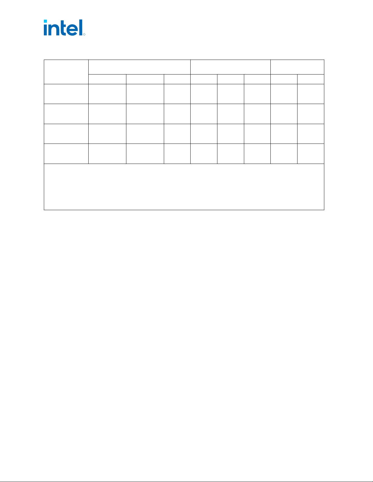
PCIe Controller
Feature
S/S Refresh/E/E Refresh /HX/HX
Refresh - Processor Line
H/H Refresh/PX - Processor
Line
P/U/U Refresh -
Processor Line
PEG10 PEG11 PEG60 PEG10 PEG60 PEG62 PEG60 PEG62
Hybrid Dual Port
Module Support
(M.2 2px2)
No No No No No No No No
Peer-2-Peer (P2P)
Mem Write
Transactions
No No Yes No No Yes Yes Yes
Peer-2-Peer (P2P)
Mem Read
Transactions
No No No No No No No No
Peer-2-Peer (P2P)
MCTP
Transactions
Yes Yes Yes Yes Yes Yes Yes Yes
1. Byte order ECN not supported
2. 4096 GB limit (Bits 63:43 always zeros)
3. Processor responds to upstream read transactions to addresses above 4096 GB (addresses where any of Bits 63:43 are
non-zero) with an Unsupported Request response. Upstream write transactions to addresses above 4096 GB will be dropped
4. SRIS is enabled in PCH PCIe RP and not in CPU PCIe RP
5. Only MSI is supported, MSI-X is not supported (no need for many vector)
6. U/U Refresh dGPU is supported but not validated
• Hierarchical PCI-compliant configuration mechanism for downstream devices.
• Traditional PCI style traffic (asynchronous snooped, PCI ordering).
• PCI Express* extended configuration space. The first 256 bytes of configuration
space aliases directly to the PCI Compatibility configuration space. The remaining
portion of the fixed 4-KB block of memory-mapped space above that (starting at
100h) is known as extended configuration space.
• PCI Express* Enhanced Access Mechanism. Accessing the device configuration
space in a flat memory-mapped fashion.
• Automatic discovery, negotiation, and training of link out of reset.
• Multiple Virtual Channel for Gen 4 port only*.
• 64-bit downstream address format, but the processor never generates an address
above 4096 GB (Bits 63:43 will always be zeros).
• 64-bit upstream address format, but the processor responds to upstream read
transactions to addresses above 4096 GB (addresses where any of Bits 63:43 are
nonzero) with an Unsupported Request response. Upstream write transactions to
addresses above 4096 GB will be dropped.
• Re-issues Configuration cycles that have been previously completed with the
Configuration Retry status.
• PCI Express* reference clock is a 100-MHz differential clock.
• Power Management Event (PME) functions.
• Modern standby
• Dynamic width capability.
• Message Signaled Interrupt (MSI and MSI-X) messages.
• Lane reversal
• Advanced Error Reporting (AER)
R
Intel
®
Core
™
, Xeon
™
6300 And Xeon
™
E 2400 Processors—PCIe* Interface
13
th
Generation Intel
®
Core
™
, Intel
®
Core
™
14
th
Generation, Intel
®
Core
™
Processor (Series 1) and (Series 2), Intel
®
Xeon
™
E
2400 Processor and Intel
®
Xeon
™
6300 Processor
Datasheet, Volume 1 of 2 May 2025
142 Doc. No.: 743844, Rev.: 015
• MCTP VDM tunneling.
• ACS - Access control services
• Precision Time Measurement (PTM) - This feature is supported on PEG60/62 with
the exception of ECN for byte ordering of the PTM value not being supported.
PEG10/11 do support ECN for byte ordering
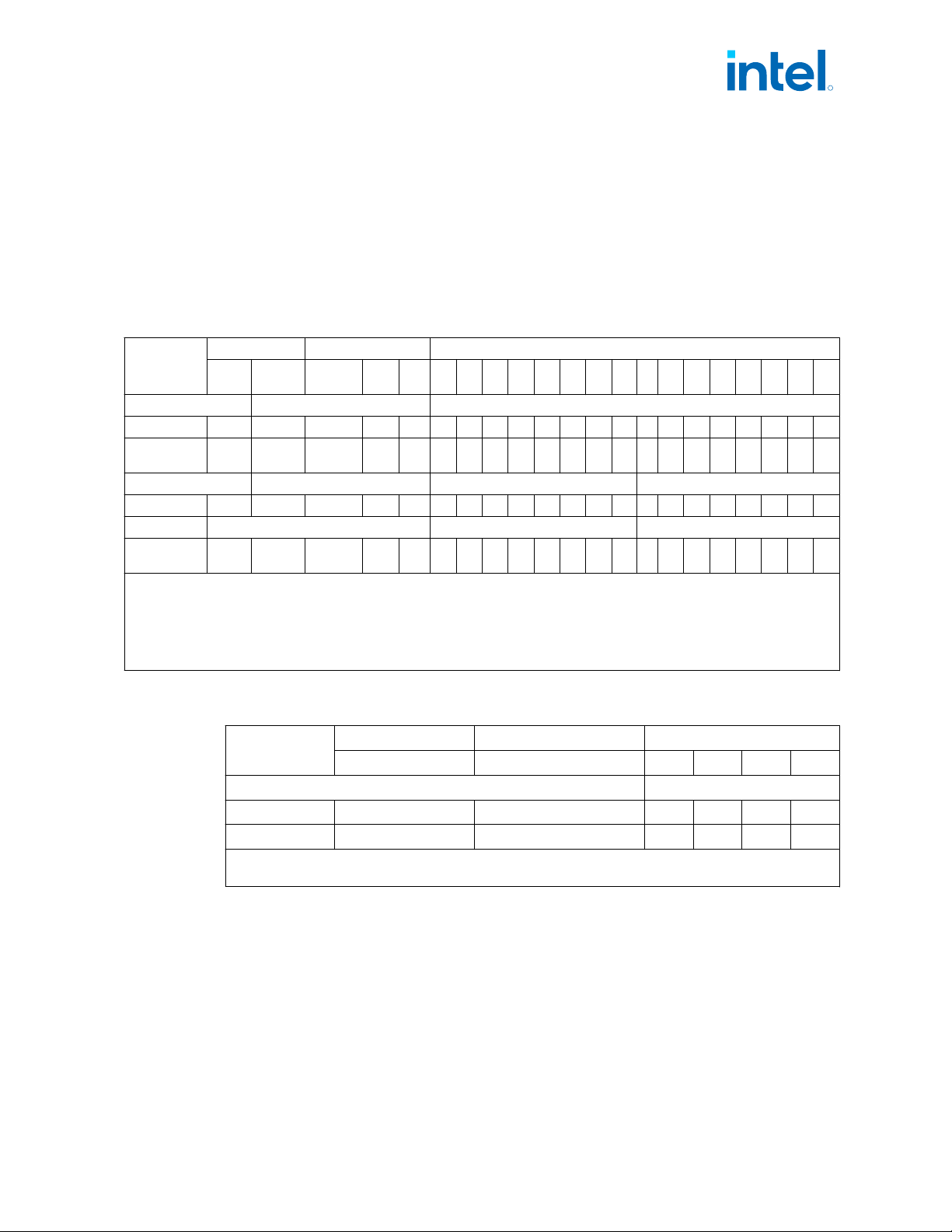
The S/S Refresh/E/E Refresh /HX/HX Refresh processor supports the configurations
shown in the following tables:
Table 51. PCI Express* 16 - Lane Bifurcation and Lane Reversal Mapping
Bifurcation
Link Width CFG Signals Lanes
0:1:0 0:1:1
CFG
[6]
CFG
[5]
CFG
[2]
0 1 2 3 4 5 6 7 8 9 10 11 12 13 14 15
PCIe controller PCIe 010 (PEG10)
1x16 x16 N/A 1 1 1 0 1 2 3 4 5 6 7 8 9 10 11 12 13 14 15
1x16
Reversed
x16 N/A 1 1 0 15 14 13 12 11 10 9 8 7 6 5 4 3 2 1 0
PCIe controller PCIe 010 (PEG10) PCIe 011 (PEG11)
2x8 x8 x8 1 0 1 0 1 2 3 4 5 6 7 0 1 2 3 4 5 6 7
PCIe controller PCIe 011 (PEG11) PCIe 010 (PEG10)
2x8
Reversed
x8 x8 1 0 0 7 6 5 4 3 2 1 0 7 6 5 4 3 2 1 0
Notes: 1. For CFG bus details, refer to Reset and Miscellaneous Signals on page 175.
2. Support is also provided for narrow width and use devices with lower number of lanes (that is, usage on x4 configuration), however further
bifurcation is not supported.
3. In case that more than one device is connected, the device with the highest lane count, should always be connected to the lower lanes, as follows:
a. Connect lane 0 of 1st device to lane 0.
b. Connect lane 0 of 2nd device to lane 8.
4. For reversal lanes, for example: When using 1x8, the 8 lane device should use lanes 8:15, so lane 15 will be connected to lane 0 of the Device.
Table 52. S/S Refresh/E/E Refresh /HX/HX Refresh - Processor PCI Express* 4 - Lane
Reversal Mapping
Bifurcation
Link Width CFG Signals Lanes
0:6:0 CFG [14] 0 1 2 3
PCIe controller PCIe 060 (PEG60)
1x4 x4 1 0 1 2 3
1x4 Reversed x4 0 3 2 1 0
Note: PCIe* Port60 is a single x4 port without bifurcation capabilities, thus bifurcation pin straps are not
applicable.
The H/H Refresh/PX processor lines supports the configurations shown in the following
tables:
R
PCIe* Interface—Intel
®
Core
™
, Xeon
™
6300 And Xeon
™
E 2400 Processors
13
th
Generation Intel
®
Core
™
, Intel
®
Core
™
14
th
Generation, Intel
®
Core
™
Processor (Series 1) and (Series 2), Intel
®
Xeon
™
E
2400 Processor and Intel
®
Xeon
™
6300 Processor
May 2025 Datasheet, Volume 1 of 2
Doc. No.: 743844, Rev.: 015 143
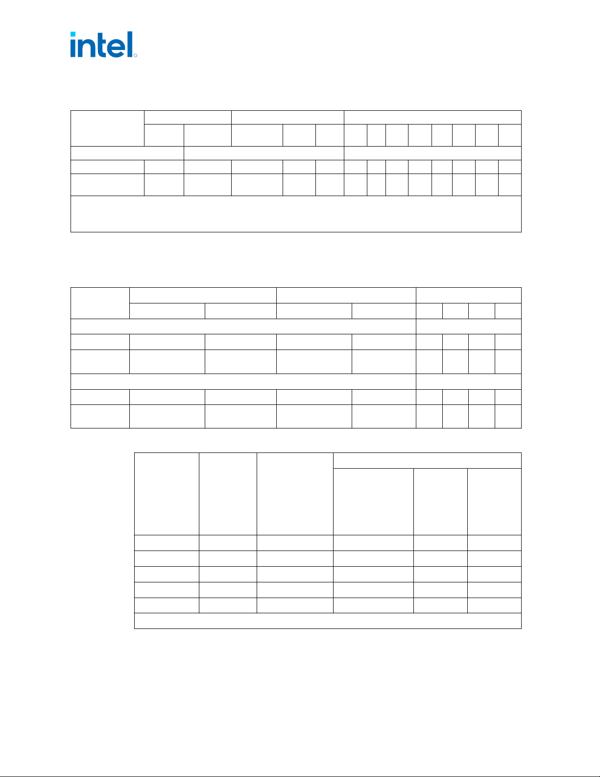
Table 53. H/H Refresh/PX PCI Express* 8 - Lane Reversal Mapping
Bifurcation
Link Width CFG Signals Lanes
0:1:0 0:1:1
CFG
[6]
CFG
[5]
CFG
[2]
0 1 2 3 4 5 6 7
PCIe controller PCIe 010 (PEG10)
1x8 x8 N/A 1 1 1 0 1 2 3 4 5 6 7
1x8
Reversed
x8 N/A 1 1 0 7 6 5 4 3 2 1 0
Notes: 1. For CFG bus details, refer to
Reset and Miscellaneous Signals on page 175.
2. Support is also provided for narrow width and use devices with lower number of lanes (that is, usage on x4 configuration), however further
bifurcation is not supported.
3. For reversal lanes, for example: When using 1x4, the 4 lane device should use lanes 4:7, so lane 7 will be connected to lane 0 of the Device.
The H/H Refresh/PX/P/U/U Refresh processor Lines supports the configurations shown
in the following tables:
Table 54. H/H Refresh/PX/P/U/U Refresh PCI Express* 4 - Lane Reversal Mapping
Bifurcation
Link Width CFG Signals Lanes
0:6:0 0:6:2 CFG [14] CFG [15] 0 1 2 3
PCIe Controller PCIe 060 (PEG60)
1x4 x4 NA 1 NA 0 1 2 3
1x4
Reversed
x4 NA 0 NA 3 2 1 0
PCIe Controller PCIe 062 (PEG62)
1x4 NA x4 NA 1 0 1 2 3
1x4
Reversed
NA x4 NA 0 3 2 1 0
Table 55. PCI Express* Maximum Transfer Rates and Theoretical Bandwidth
PCI Express*
Generation
Encoding
Maximum
Transfer Rate
[GT/s]
Theoretical Bandwidth [GB/s]
S/S
Refresh/E/H/H
Refresh/HX/HX
Refresh /P/U/U
Refresh
x4
S/S
Refresh/E/
H/H
Refresh/H
X/HX
Refresh
x8
S/S
Refresh/E/
HX/HX
Refresh
x16
Gen 1 8b/10b 2.5 1.0 2.0 4.0
Gen 2 8b/10b 5 2.0 4.0 8.0
Gen 3 128b/130b 8 3.9 7.9 15.8
Gen 4 128b/130b 16 7.9 15.8 31.5
Gen 5 128b/130b 32
1
15.8
1
31.5
1
63
1
Note: 1. Transfer rate and max theoretical Bandwidth are not final and could be lowered.
The above table summarizes the transfer rates and theoretical bandwidth of PCI
Express* link.
R
Intel
®
Core
™
, Xeon
™
6300 And Xeon
™
E 2400 Processors—PCIe* Interface
13
th
Generation Intel
®
Core
™
, Intel
®
Core
™
14
th
Generation, Intel
®
Core
™
Processor (Series 1) and (Series 2), Intel
®
Xeon
™
E
2400 Processor and Intel
®
Xeon
™
6300 Processor
Datasheet, Volume 1 of 2 May 2025
144 Doc. No.: 743844, Rev.: 015