743844-015.pdf - 第129页
Supported technologies : DDR4, DDR5, LPDDR4x and LPDDR5/x. Refresh Management (RFM) RFM is supported according to JEDEC spec. LPDDR5/x: RFM feature is enabled. DDR5: RFM feature is not yet enabled. Integrated Memory Cont…
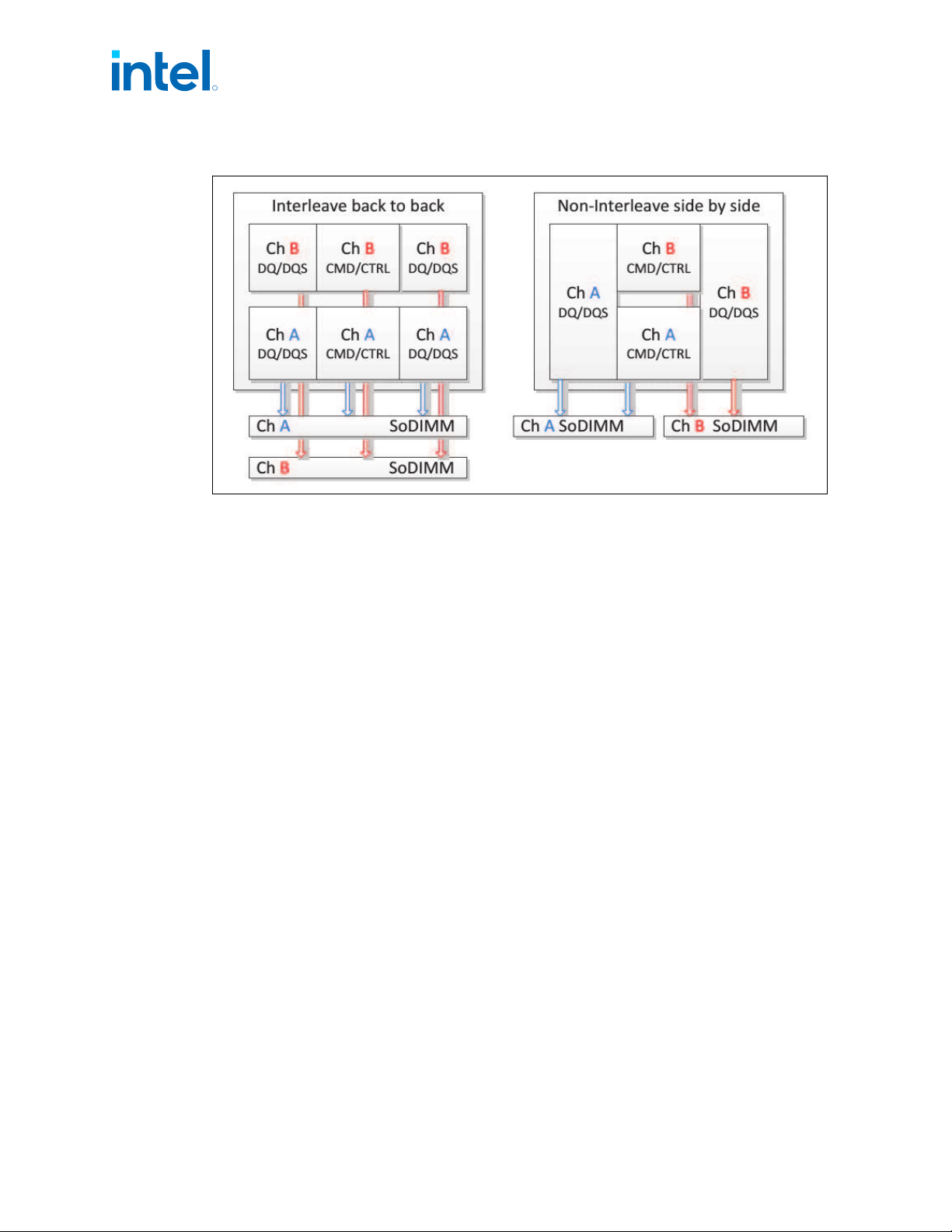
Figure 20. DDR4 Interleave (IL) and Non-Interleave (NIL) Modes Mapping
DRAM Clock Generation
Each support rank has a differential clock pair for DDR4/5. Each sub-channel has a
differential clock pair for LPDDR4x. Each sub-channel has a (CK_P/N and WCK_P/N)
differential clock pair for LPDDR5/x.
DRAM Reference Voltage Generation
Read Vref is generated by the memory controller in all technologies. Write Vref is
generated by the DRAM in all technologies. Command Vref is generated by the DRAM
in LPDDR4x/5 while the memory controller generates VrefCA per DIMM for DDR4. In
all cases, it has small step sizes and is trained by MRC.
Data Swizzling
All Processor Lines does not have die-to-package DDR swizzling.
Error Correction With Standard RAM
In-Band error-correcting code (IBECC) correct single-bit memory errors in standard,
non-ECC memory.
Supported only in Chrome systems.
Post Package Repair
PPR is supported according to Jedec Spec.
BIOS can identify a single Row failure per Bank in DRAM and perform Post Package
Repair (PPR) to exchange failing Row with spare Row.
PPR can be supported only with DRAM that supports PPR according to Jedec spec.
5.1.15
5.1.16
5.1.17
5.1.18
5.1.19
R
Intel
®
Core
™
, Xeon
™
6300 And Xeon
™
E 2400 Processors—Memory
13
th
Generation Intel
®
Core
™
, Intel
®
Core
™
14
th
Generation, Intel
®
Core
™
Processor (Series 1) and (Series 2), Intel
®
Xeon
™
E
2400 Processor and Intel
®
Xeon
™
6300 Processor
Datasheet, Volume 1 of 2 May 2025
128 Doc. No.: 743844, Rev.: 015

Supported technologies : DDR4, DDR5, LPDDR4x and LPDDR5/x.
Refresh Management (RFM)
RFM is supported according to JEDEC spec.
LPDDR5/x: RFM feature is enabled.
DDR5: RFM feature is not yet enabled.
Integrated Memory Controller (IMC) Power Management
The main memory is power managed during normal operation and in low-power ACPI
C-states.
Disabling Unused System Memory Outputs
Any system memory (SM) interface signal that goes to a memory in which it is not
connected to any actual memory devices (such as SODIMM connector is unpopulated,
or is single-sided) is tri-stated. The benefits of disabling unused SM signals are:
• Reduced power consumption.
• Reduced possible overshoot/undershoot signal quality issues seen by the
processor I/O buffer receivers caused by reflections from potentially unterminated
transmission lines.
When a given rank is not populated, the corresponding control signals (CLK_P/
CLK_N/CKE/ODT/CS) are not driven.
At reset, all rows should be assumed to be populated, until it can be proven that they
are not populated. This is due to the fact that when CKE is tri-stated with a DRAMs
present, the DRAMs are not ensured to maintain data integrity. CKE tri-state should be
enabled by BIOS where appropriate, since at reset all rows should be assumed to be
populated.
DRAM Power Management and Initialization
The processor implements extensive support for power management on the memory
interface. Each channel drives 4 CKE pins, one per rank.
The CKE is one of the power-saving means. When CKE is off, the internal DDR clock is
disabled and the DDR power is reduced. The power-saving differs according to the
selected mode and the DDR type used. For more information, refer to the IDD table in
the DDR specification.
The processor supports four different types of power-down modes in package C0
state. The different power-down modes can be enabled through configuring PM PDWN
config register. The type of CKE power-down can be configured through PDWN_mode
(bits 15:12) and the idle timer can be configured through PDWN_idle_counter (bits
11:0).
The different power-down modes supported are:
• No power-down: (CKE disable)
5.1.20
5.2
5.2.1
5.2.2
R
Memory—Intel
®
Core
™
, Xeon
™
6300 And Xeon
™
E 2400 Processors
13
th
Generation Intel
®
Core
™
, Intel
®
Core
™
14
th
Generation, Intel
®
Core
™
Processor (Series 1) and (Series 2), Intel
®
Xeon
™
E
2400 Processor and Intel
®
Xeon
™
6300 Processor
May 2025 Datasheet, Volume 1 of 2
Doc. No.: 743844, Rev.: 015 129

• Active Power-down (APD): This mode is entered if there are open pages when
de-asserting CKE. In this mode the open pages are retained. Power-saving in this
mode is the lowest. Power consumption of DDR is defined by IDD3P. Exiting this
mode is fined by tXP – a small number of cycles.
• Pre-charged Power-down (PPD): This mode is entered if all banks in DDR are
pre-charged when de-asserting CKE. Power-saving in this mode is intermediate –
better than APD. Power consumption is defined by IDD2P. Exiting this mode is
defined by tXP. The difference from APD mode is that when waking-up, all page-
buffers are empty.)
*APD is default in P and U Processor line, otherwise it's "No Power down".
The CKE is determined per rank, whenever it is inactive. Each rank has an idle
counter. The idle-counter starts counting as soon as the rank has no accesses, and if it
expires, the rank may enter power-down while no new transactions to the rank arrive
to queues. The idle-counter begins counting at the last incoming transaction arrival. It
is important to understand that since the power-down decision is per rank, the IMC
can find many opportunities to power down ranks, even while running memory
intensive applications; the savings are significant (may be few Watts, according to
DDR specification). This is significant when each channel is populated with more
ranks.
Selection of power modes should be according to power-performance or a thermal
trade-off of a given system:
• When trying to achieve maximum performance and power or thermal
consideration is not an issue: use no power-down
• In a system which tries to minimize power-consumption, try using the deepest
power-down mode possible
• In high-performance systems with dense packaging (that is, tricky thermal
design) the power-down mode should be considered in order to reduce the heating
and avoid DDR throttling caused by the heating.
The idle timer expiration count defines the # of DCLKs that a rank is idle that causes
entry to the selected power mode. As this timer is set to a shorter time the IMC will
have more opportunities to put the DDR in power-down. There is no BIOS hook to set
this register. Customers choosing to change the value of this register can do it by
changing it in the BIOS. For experiments, this register can be modified in real time if
BIOS does not lock the IMC registers.
Initialization Role of CKE
During power-up, CKE is the only input to the SDRAM that has its level recognized
(other than the reset pin) once power is applied. It should be driven LOW by the DDR
controller to make sure the SDRAM components float DQ and DQS during power-up.
CKE signals remain LOW (while any reset is active) until the BIOS writes to a
configuration register. Using this method, CKE is ensured to remain inactive for much
longer than the specified 200 micro-seconds after power and clocks to SDRAM devices
are stable. In LPDDR5/DDR5, there is no CKE pin and the power management roll is
assumed by the CS signals.
5.2.2.1
R
Intel
®
Core
™
, Xeon
™
6300 And Xeon
™
E 2400 Processors—Memory
13
th
Generation Intel
®
Core
™
, Intel
®
Core
™
14
th
Generation, Intel
®
Core
™
Processor (Series 1) and (Series 2), Intel
®
Xeon
™
E
2400 Processor and Intel
®
Xeon
™
6300 Processor
Datasheet, Volume 1 of 2 May 2025
130 Doc. No.: 743844, Rev.: 015