743844-015.pdf - 第215页
Symbol Definition and Conditions Minimum Maximum Units Notes 1 C pad Pad Capacitance 0.7 1.8 pF - Ileak000 leakage current @ 0 V — 0.25 mA - Ileak100 leakage current @ Vcc 1p05 — 0.15 mA - Notes: 1. Vcc 1p05_PROC supplie…
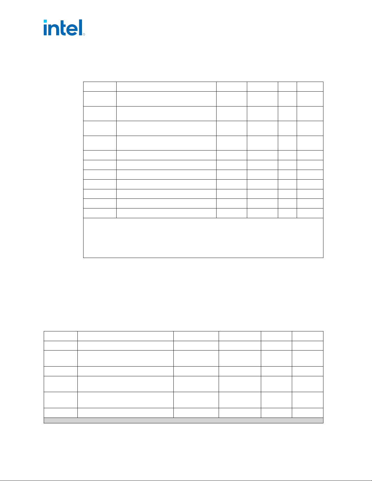
GTL and OD DC Specification
Table 95. GTL Signal Group and Open Drain Signal Group DC Specifications
Symbol Parameter Minimum Maximum Units Notes
1
V
IL
Input Low Voltage (TAP, except
PROC_JTAG_TCK, PROC_JTAG_TRST#)
— 0.6*Vcc V 2, 5
V
IH
Input High Voltage (TAP, except
PROC_JTAG_TCK, PROC_JTAG_TRST#)
0.72*Vcc — V 2, 4, 5
V
IL
Input Low Voltage
(PROC_JTAG_TCK,PROC_JTAG_TRST#)
— 0.3*Vcc V 2, 5
V
IH
Input High Voltage
(PROC_JTAG_TCK,PROC_JTAG_TRST#)
0.7*Vcc — V 2, 4, 5
V
HYSTERESIS
Hysteresis Voltage 0.2*Vcc — V -
R
ON
Buffer on Resistance (TDO) 7 17 Ω -
V
IL
Input Low Voltage (other GTL) — 0.6*Vcc V 2, 5
V
IH
Input High Voltage (other GTL) 0.72*Vcc — V 2, 4, 5
R
ON
Buffer on Resistance (BPM) 12 28 Ω -
R
ON
Buffer on Resistance (other GTL) 16 24 Ω -
I
LI
Input Leakage Current — ±150 μA 3
Notes: 1. All specifications in this table apply to all processor frequencies.
2. The Vcc referred to in these specifications refers to instantaneous Vcc1p05_PROC/IO.
3. For V
IN
between 0 V and Vcc. Measured when the driver is tri-stated.
4. V
IH
and V
OH
may experience excursions above Vcc. However, input signal drivers should
comply with the signal quality specifications.
5. Refer to the processor I/O Buffer Models for I/V characteristics.
PECI DC Characteristics
The PECI interface operates at a nominal voltage set by Vcc
1p05_PROC
. The set of DC
electrical specifications shown in the following table is used with devices normally
operating from a Vcc
1P05_PROC
interface supply.
Vcc
1p05_PROC
nominal levels will vary between processor families. All PECI devices will
operate at the Vcc
1p05_PROC
level determined by the processor installed in the system.
Table 96. PECI DC Electrical Limits
Symbol Definition and Conditions Minimum Maximum Units Notes
1
R
up
Internal pull up resistance 15 45 Ω 3
V
in
Input Voltage Range
-0.15
Vcc1p05_PROC
+ 0.15
V -
V
hysteresis
Hysteresis 0.1 * Vcc
1p05_PROC
— V -
V
IL
Input Voltage Low- Edge Threshold
Voltage
0.275 *
Vcc
1p05_PROC
0.525 *
Vcc1p05_PROC
V -
V
IH
Input Voltage High- Edge Threshold
Voltage
0.550 *
Vcc
1p05_PROC
0.725
*Vcc1p05_PROC
V -
C
bus
Bus Capacitance per Node — 10 pF -
continued...
13.2.2.9
13.2.2.10
R
Intel
®
Core
™
, Xeon
™
6300 And Xeon
™
E 2400 Processors—Electrical Specifications
13
th
Generation Intel
®
Core
™
, Intel
®
Core
™
14
th
Generation, Intel
®
Core
™
Processor (Series 1) and (Series 2), Intel
®
Xeon
™
E
2400 Processor and Intel
®
Xeon
™
6300 Processor
Datasheet, Volume 1 of 2 May 2025
214 Doc. No.: 743844, Rev.: 015
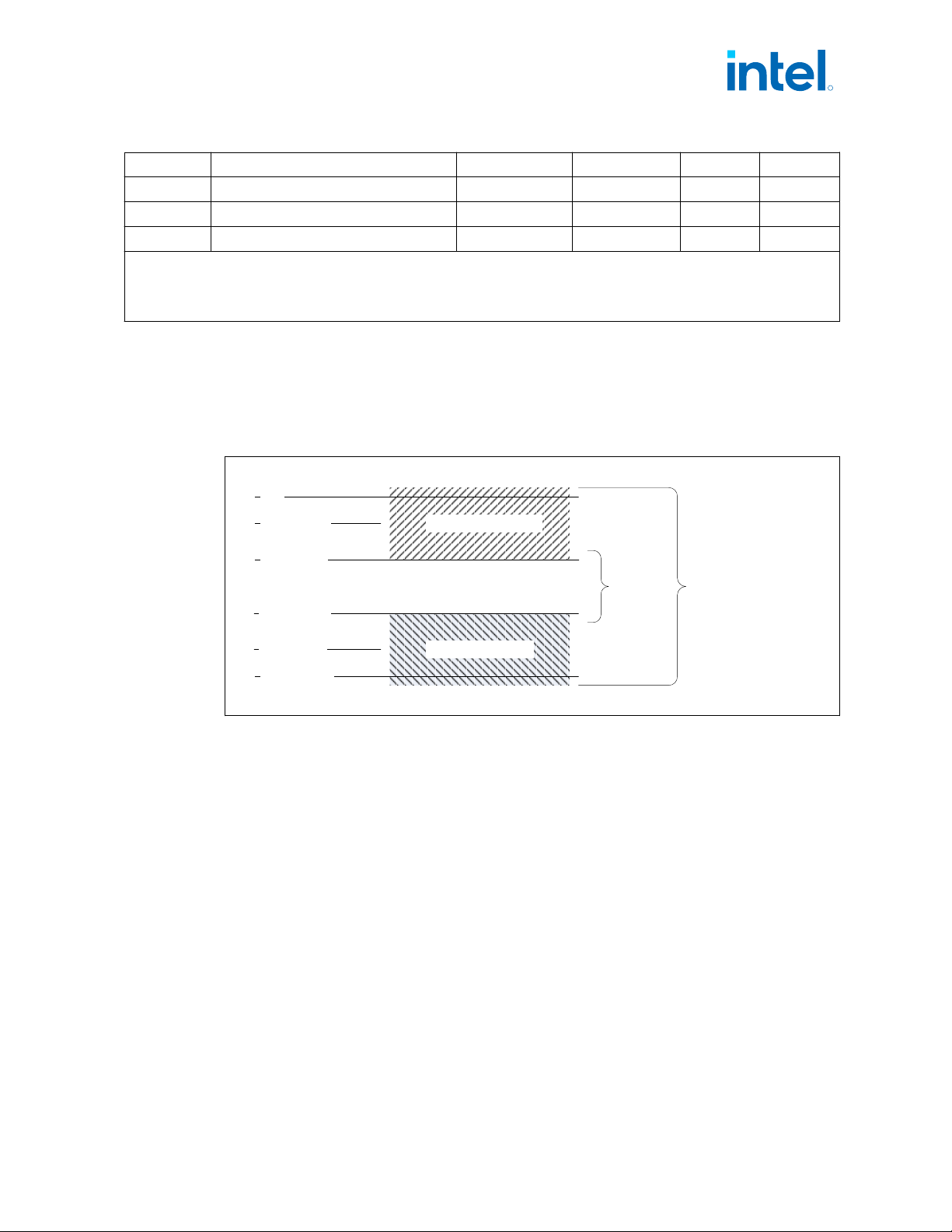
Symbol Definition and Conditions Minimum Maximum Units Notes
1
C
pad
Pad Capacitance 0.7 1.8 pF -
Ileak000 leakage current @ 0 V — 0.25 mA -
Ileak100 leakage current @ Vcc
1p05
— 0.15 mA -
Notes: 1. Vcc
1p05_PROC
supplies the PECI interface. PECI behavior does not affect Vcc
1p05_PROC
minimum / maximum
specifications.
2. The leakage specification applies to powered devices on the PECI bus.
3. The PECI buffer internal pull up resistance measured at 0.75* Vcc
1p05_PROC
.
Input Device Hysteresis
The input buffers in both client and host models should use a Schmitt-triggered input
design for improved noise immunity. Use the following figure as a guide for input
buffer design.
Figure 27. Input Device Hysteresis
Minimum V
P
Maximum V
P
Minimum V
N
Maximum V
N
PECI High Range
PECI Low Range
Valid Input
Signal Range
Minimum
Hysteresis
V
TTD
PECI Ground
R
Electrical Specifications—Intel
®
Core
™
, Xeon
™
6300 And Xeon
™
E 2400 Processors
13
th
Generation Intel
®
Core
™
, Intel
®
Core
™
14
th
Generation, Intel
®
Core
™
Processor (Series 1) and (Series 2), Intel
®
Xeon
™
E
2400 Processor and Intel
®
Xeon
™
6300 Processor
May 2025 Datasheet, Volume 1 of 2
Doc. No.: 743844, Rev.: 015 215
14.0 Package Mechanical Specifications
Package Mechanical Attributes
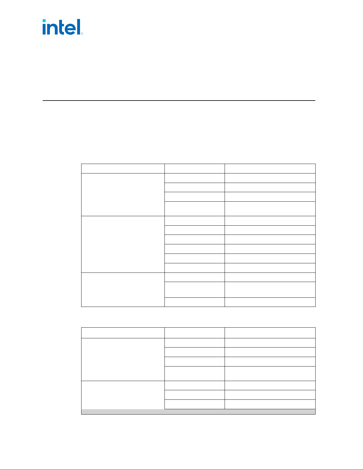
The S/S refresh Processor Lines use a Flip Chip technology available in a Land Grid
Array (LGA) package. The following table provides an overview of the package
mechanical attributes. For specific dimensions (die size, die location, and so on), refer
to the processor package mechanical drawings.
Table 97. S/S Refresh/E/E Refresh LGA Processor Package Mechanical Attributes
Package Parameter S LGA Processor Lines
Package Technology
Package Type Flip Chip Land Grid Array
Interconnect Land Grid Array (LGA)
Lead Free N/A
Halogenated Flame
Retardant Free
Yes
Package Configuration
Solder Ball Composition N/A
Ball/Pin Count 1700
Grid Array Pattern Grid Array
Land Side Capacitors Yes
Die Side Capacitors Yes
Die Configuration Single Die Single-Chip Package with HIS
Package Dimensions
Nominal Package Size 45.0 x 37.5 mm
Z
Substrate Z=1.116 mm +/-0.95
Die Z is 0.37 mm
Minimum Ball/Pin pitch 0.8 mm
Table 98. HX BGA Processor Package Mechanical Attributes
Package Parameter
HX Processor Lines
Package Technology
Package Type Flip Chip Ball Grid Array
Interconnect Ball Grid Array (BGA)
Lead Free N/A
Halogenated Flame
Retardant Free
Yes
Package Configuration
Solder Ball Composition Yes
Ball/Pin Count 1964
Grid Array Pattern Grid Array
continued...
14.1
R
Intel
®
Core
™
, Xeon
™
6300 And Xeon
™
E 2400 Processors—Package Mechanical Specifications
13
th
Generation Intel
®
Core
™
, Intel
®
Core
™
14
th
Generation, Intel
®
Core
™
Processor (Series 1) and (Series 2), Intel
®
Xeon
™
E
2400 Processor and Intel
®
Xeon
™
6300 Processor
Datasheet, Volume 1 of 2 May 2025
216 Doc. No.: 743844, Rev.: 015