743844-015.pdf - 第167页
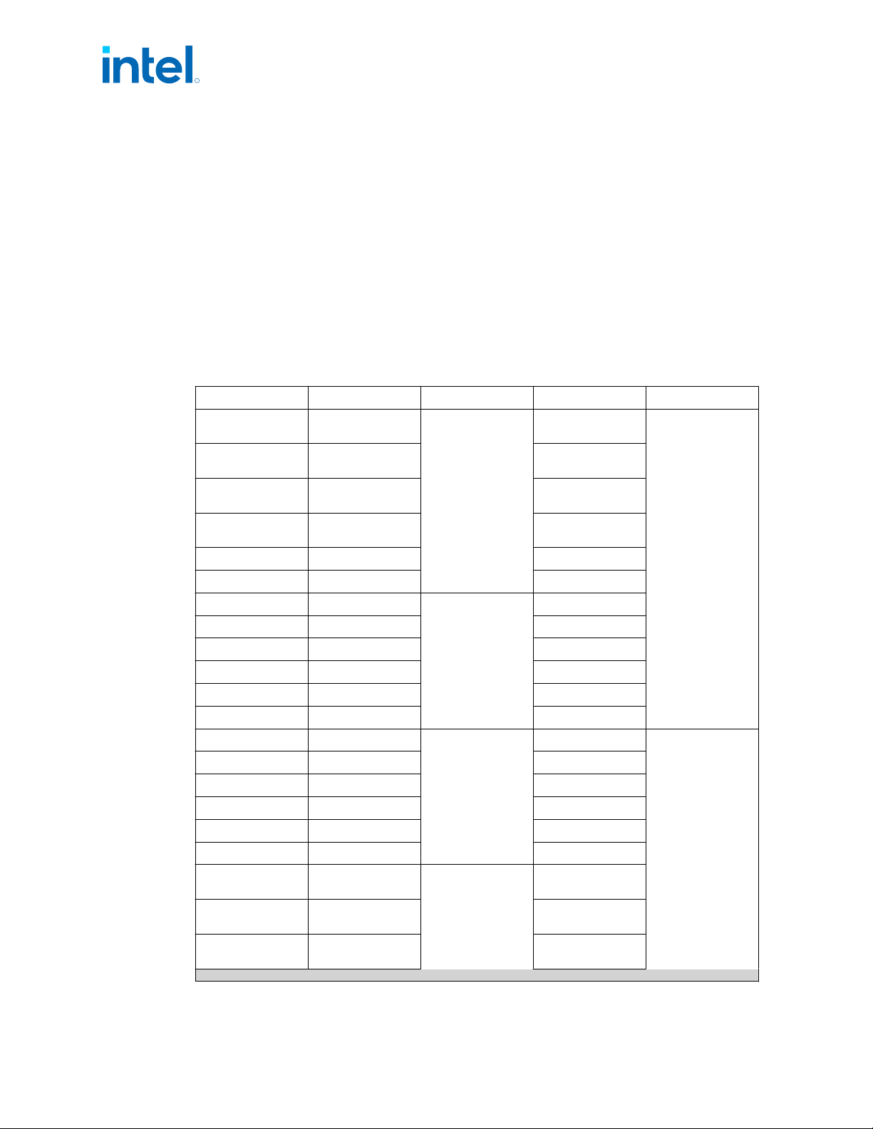
Pin Name Option 1 CFG Option 2 CFG CSI_A_DN[0] / CSI_B_DN[3] CSI_A_DN[0] CSI_B_DN[3] CSI_A_CLK_P CSI_A_CLK_P Not Used CSI_A_CLK_N CSI_A_CLK_N Not Used Table 68. PX CSI-2 Lane Allocation Table Pin Name Option 1 CFG Option…
Camera Control Logic
The camera infrastructure supports several architectural options for camera control
utilizing camera PMIC and/or discrete logic. IPU6 control options utilize I
2
C for
bidirectional communication and PCH GPIOs to drive various control functions.
Camera Modules
Intel maintains an Intel User Facing Camera Approved Vendor List and Intel World-
Facing Approved Vendor List to simplify system design. Additional services are
available to support non-AVL options.
CSI-2 Lane Configurations
Table 67. H/H Refresh/P/U/U Refresh CSI-2 Lane Allocation Table
Pin Name Option 1 CFG Option 2 CFG
CSI_D_DP[1] /
CSI_C_DP[2]
CSI_D_DP[1] X2 CSI_C_DP[2] X4
CSI_D_DN[1] /
CSI_C_DN[2]
CSI_D_DN[1] CSI_C_DN[2]
CSI_D_DP[0] /
CSI_C_DP[3]
CSI_D_DP[0] CSI_C_DP[3]
CSI_D_DN[0] /
CSI_C_DN[3]
CSI_D_DN[0] CSI_C_DN[3]
CSI_D_CLK_P CSI_D_CLK_P Not used
CSI_D_CLK_N CSI_D_CLK_N Not Used
CSI_C_DP[1] CSI_C_DP[1] X2 CSI_C_DP[1]
CSI_C_DN[1] CSI_C_DN[1] CSI_C_DN[1]
CSI_C_DP[0] CSI_C_DP[0] CSI_C_DP[0]
CSI_C_DN[0] CSI_C_DN[0] CSI_C_DN[0]
CSI_C_CLK_P CSI_C_CLK_P CSI_C_CLK_P
CSI_C_CLK_N CSI_C_CLK_N CSI_C_CLK_N
CSI_B_DP[1] CSI_B_DP[1] X2 CSI_B_DP[1] X4
CSI_B_DN[1] CSI_B_DN[1] CSI_B_DN[1]
CSI_B_DP[0] CSI_B_DP[0] CSI_B_DP[0]
CSI_B_DN[0] CSI_B_DN[0] CSI_B_DN[0]
CSI_B_CLK_P CSI_B_CLK_P CSI_B_CLK_P
CSI_B_CLK_N CSI_B_CLK_N CSI_B_CLK_N
CSI_A_DP[1] /
CSI_B_DP[2]
CSI_A_DP[1] X2 CSI_B_DP[2]
CSI_A_DN[1] /
CSI_B_DN[2]
CSI_A_DN[1] CSI_B_DN[2]
CSI_A_DP[0] /
CSI_B_DP[3]
CSI_A_DP[0] CSI_B_DP[3]
continued...
11.2.1
11.2.2
11.2.3
R
Intel
®
Core
™
, Xeon
™
6300 And Xeon
™
E 2400 Processors—Camera/MIPI
13
th
Generation Intel
®
Core
™
, Intel
®
Core
™
14
th
Generation, Intel
®
Core
™
Processor (Series 1) and (Series 2), Intel
®
Xeon
™
E
2400 Processor and Intel
®
Xeon
™
6300 Processor
Datasheet, Volume 1 of 2 May 2025
166 Doc. No.: 743844, Rev.: 015
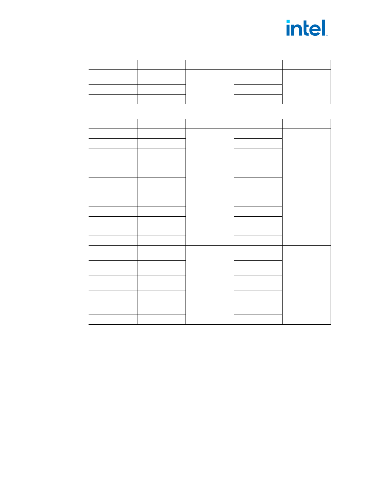
Pin Name Option 1 CFG Option 2 CFG
CSI_A_DN[0] /
CSI_B_DN[3]
CSI_A_DN[0] CSI_B_DN[3]
CSI_A_CLK_P CSI_A_CLK_P Not Used
CSI_A_CLK_N CSI_A_CLK_N Not Used
Table 68. PX CSI-2 Lane Allocation Table
Pin Name Option 1 CFG Option 2 CFG
CSI_C_DP[1] CSI_C_DP[1]
X2
CSI_C_DP[1]
X2
CSI_C_DN[1] CSI_C_DN[1] CSI_C_DN[1]
CSI_C_DP[0] CSI_C_DP[0] CSI_C_DP[0]
CSI_C_DN[0] CSI_C_DN[0] CSI_C_DN[0]
CSI_C_CLK_P CSI_C_CLK_P CSI_C_CLK_P
CSI_C_CLK_N CSI_C_CLK_N CSI_C_CLK_N
CSI_B_DP[1] CSI_B_DP[1]
X2
CSI_B_DP[1]
X4
CSI_B_DN[1] CSI_B_DN[1] CSI_B_DN[1]
CSI_B_DP[0] CSI_B_DP[0] CSI_B_DP[0]
CSI_B_DN[0] CSI_B_DN[0] CSI_B_DN[0]
CSI_B_CLK_P CSI_B_CLK_P CSI_B_CLK_P
CSI_B_CLK_N CSI_B_CLK_N CSI_B_CLK_N
CSI_A_DP[1] /
CSI_B_DP[2]
CSI_A_DP[1]
X2
CSI_B_DP[2]
X4
CSI_A_DN[1] /
CSI_B_DN[2]
CSI_A_DN[1] CSI_B_DN[2]
CSI_A_DP[0] /
CSI_B_DP[3]
CSI_A_DP[0] CSI_B_DP[3]
CSI_A_DN[0] /
CSI_B_DN[3]
CSI_A_DN[0] CSI_B_DN[3]
CSI_A_CLK_P CSI_A_CLK_P Not Used
CSI_A_CLK_N CSI_A_CLK_N Not Used
R
Camera/MIPI—Intel
®
Core
™
, Xeon
™
6300 And Xeon
™
E 2400 Processors
13
th
Generation Intel
®
Core
™
, Intel
®
Core
™
14
th
Generation, Intel
®
Core
™
Processor (Series 1) and (Series 2), Intel
®
Xeon
™
E
2400 Processor and Intel
®
Xeon
™
6300 Processor
May 2025 Datasheet, Volume 1 of 2
Doc. No.: 743844, Rev.: 015 167
12.0 Signal Description
This chapter describes the processor signals. They are arranged in functional groups
according to their associated interface or category. The notations in the following table
are used to describe the signal type.
The signal description also includes the type of buffer used for the particular signal
(refer to the following table).
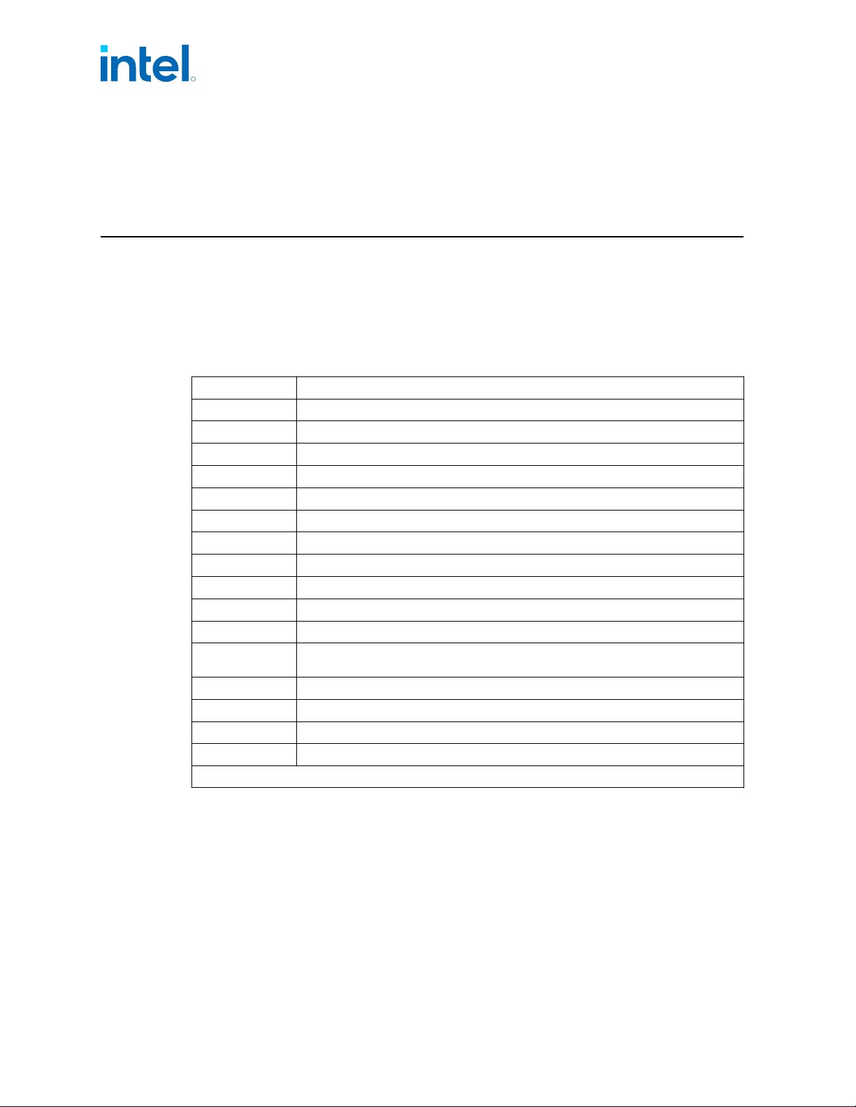
Table 69. Signal Tables Terminology
Notation Signal Type
I Input pin
O Output pin
I/O Input/Output, Bi-directional pin
SE Single Ended Link
Diff Differential Link
CMOS CMOS buffers. 1.05 V- tolerant
OD Open Drain buffer
LPDDR4x LPDDR4x buffers: 1.1 V-tolerant
LPDDR5 LPDDR5 buffers
DDR4 DDR4 buffers: 1.2 V-tolerant
DDR5 DDR5 buffers: 1.1 V-tolerant
A
Analog reference or output. May be used as a threshold voltage or for buffer
compensation
GTL Gunning Transceiver Logic signaling technology
Ref Voltage Reference signal
Availability Signal Availability condition - based on segment, SKU, platform type or any other factor
Asynchronous 1 Signal has no timing relationship with any reference clock.
Note: Qualifier for a buffer type.
R
Intel
®
Core
™
, Xeon
™
6300 And Xeon
™
E 2400 Processors—Signal Description
13
th
Generation Intel
®
Core
™
, Intel
®
Core
™
14
th
Generation, Intel
®
Core
™
Processor (Series 1) and (Series 2), Intel
®
Xeon
™
E
2400 Processor and Intel
®
Xeon
™
6300 Processor
Datasheet, Volume 1 of 2 May 2025
168 Doc. No.: 743844, Rev.: 015