743844-015.pdf - 第166页
Camera Control Logic The camera infr astructure supports sever al architectural options for camer a control utilizing camera PMIC and/or discrete logic. IPU6 control options utilize I 2 C for bidirectional communication …

11.0 Camera/MIPI
Camera/MIPI is supported on the following processor line.
• P/PX-Processor line
• H/H Refresh-Processor line
• U/U Refresh -Processor line
NOTE
The availability of the features above may vary between different processor SKUs.
Camera Pipe Support
The IPU6se fixed function pipe supports the following functions:
• Black level correction;
• White balance;
• Color matching;
• Lens shading (vignette) correction;
• Color crosstalk (color shading) correction;
• Dynamic defect pixel replacement;
• Auto-focus-pixel (PDAF) hiding;
• High quality demosaic;
• Scaling and format conversion;
• Temporal noise reduction running on Intel graphics.
MIPI* CSI-2 Camera Interconnect
The Camera I/O Controller provides a native/integrated interconnect to camera
sensors, compliant with MIPI* CSI-2 V2.0 protocol. Total of 8 data+4 clock lanes are
available for the camera interface supporting up to 4 sensors .
Data transmission interface (referred as CSI-2) is a unidirectional differential serial
interface with data and clock signals; the physical layer of this interface is the MIPI*
Alliance Specification for D-PHY.
The control interface (referred as CCI) is a bi-directional control interface compatible
with I
2
C standard.
11.1
11.2
R
Camera/MIPI—Intel
®
Core
™
, Xeon
™
6300 And Xeon
™
E 2400 Processors
13
th
Generation Intel
®
Core
™
, Intel
®
Core
™
14
th
Generation, Intel
®
Core
™
Processor (Series 1) and (Series 2), Intel
®
Xeon
™
E
2400 Processor and Intel
®
Xeon
™
6300 Processor
May 2025 Datasheet, Volume 1 of 2
Doc. No.: 743844, Rev.: 015 165
Camera Control Logic
The camera infrastructure supports several architectural options for camera control
utilizing camera PMIC and/or discrete logic. IPU6 control options utilize I
2
C for
bidirectional communication and PCH GPIOs to drive various control functions.
Camera Modules
Intel maintains an Intel User Facing Camera Approved Vendor List and Intel World-
Facing Approved Vendor List to simplify system design. Additional services are
available to support non-AVL options.
CSI-2 Lane Configurations
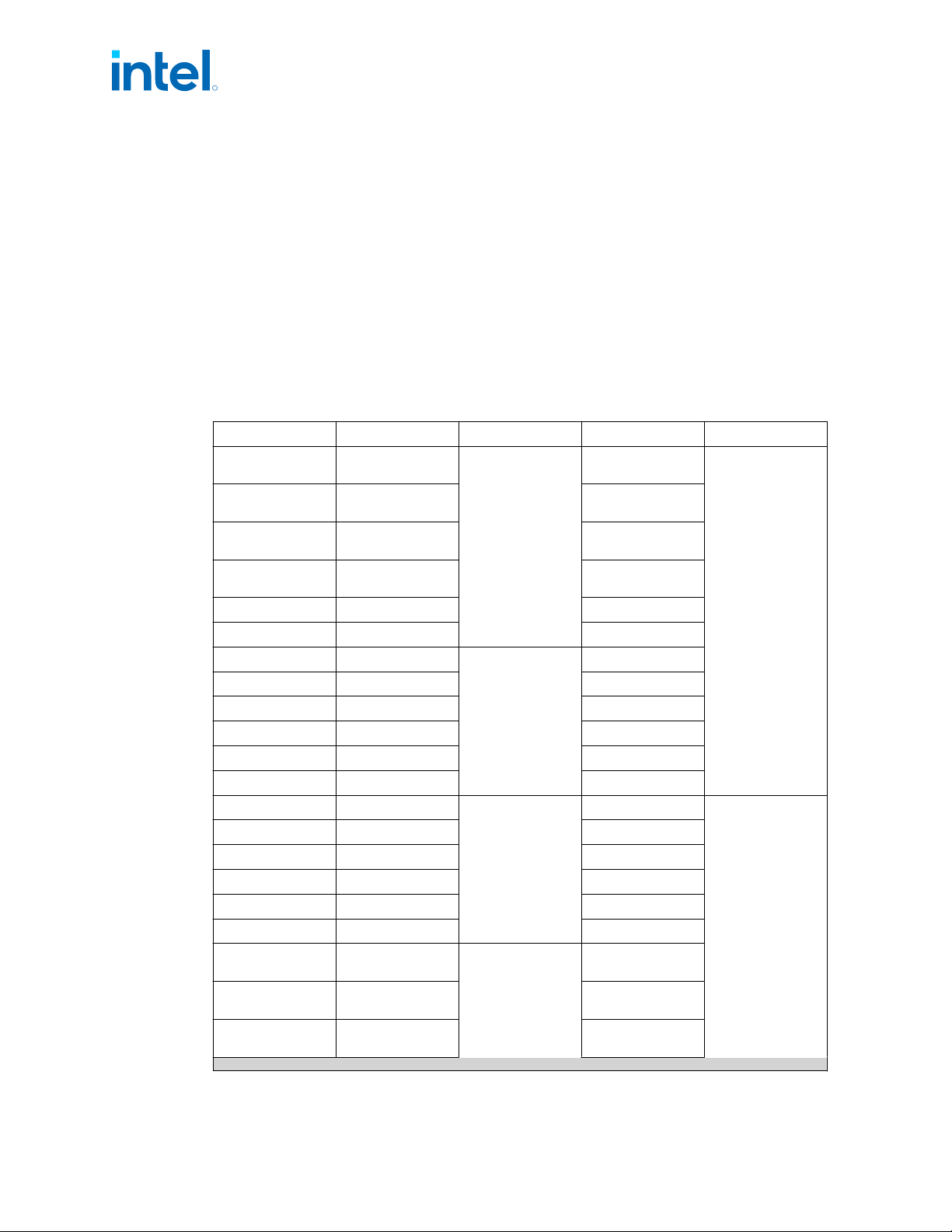
Table 67. H/H Refresh/P/U/U Refresh CSI-2 Lane Allocation Table
Pin Name Option 1 CFG Option 2 CFG
CSI_D_DP[1] /
CSI_C_DP[2]
CSI_D_DP[1] X2 CSI_C_DP[2] X4
CSI_D_DN[1] /
CSI_C_DN[2]
CSI_D_DN[1] CSI_C_DN[2]
CSI_D_DP[0] /
CSI_C_DP[3]
CSI_D_DP[0] CSI_C_DP[3]
CSI_D_DN[0] /
CSI_C_DN[3]
CSI_D_DN[0] CSI_C_DN[3]
CSI_D_CLK_P CSI_D_CLK_P Not used
CSI_D_CLK_N CSI_D_CLK_N Not Used
CSI_C_DP[1] CSI_C_DP[1] X2 CSI_C_DP[1]
CSI_C_DN[1] CSI_C_DN[1] CSI_C_DN[1]
CSI_C_DP[0] CSI_C_DP[0] CSI_C_DP[0]
CSI_C_DN[0] CSI_C_DN[0] CSI_C_DN[0]
CSI_C_CLK_P CSI_C_CLK_P CSI_C_CLK_P
CSI_C_CLK_N CSI_C_CLK_N CSI_C_CLK_N
CSI_B_DP[1] CSI_B_DP[1] X2 CSI_B_DP[1] X4
CSI_B_DN[1] CSI_B_DN[1] CSI_B_DN[1]
CSI_B_DP[0] CSI_B_DP[0] CSI_B_DP[0]
CSI_B_DN[0] CSI_B_DN[0] CSI_B_DN[0]
CSI_B_CLK_P CSI_B_CLK_P CSI_B_CLK_P
CSI_B_CLK_N CSI_B_CLK_N CSI_B_CLK_N
CSI_A_DP[1] /
CSI_B_DP[2]
CSI_A_DP[1] X2 CSI_B_DP[2]
CSI_A_DN[1] /
CSI_B_DN[2]
CSI_A_DN[1] CSI_B_DN[2]
CSI_A_DP[0] /
CSI_B_DP[3]
CSI_A_DP[0] CSI_B_DP[3]
continued...
11.2.1
11.2.2
11.2.3
R
Intel
®
Core
™
, Xeon
™
6300 And Xeon
™
E 2400 Processors—Camera/MIPI
13
th
Generation Intel
®
Core
™
, Intel
®
Core
™
14
th
Generation, Intel
®
Core
™
Processor (Series 1) and (Series 2), Intel
®
Xeon
™
E
2400 Processor and Intel
®
Xeon
™
6300 Processor
Datasheet, Volume 1 of 2 May 2025
166 Doc. No.: 743844, Rev.: 015
Pin Name Option 1 CFG Option 2 CFG
CSI_A_DN[0] /
CSI_B_DN[3]
CSI_A_DN[0] CSI_B_DN[3]
CSI_A_CLK_P CSI_A_CLK_P Not Used
CSI_A_CLK_N CSI_A_CLK_N Not Used
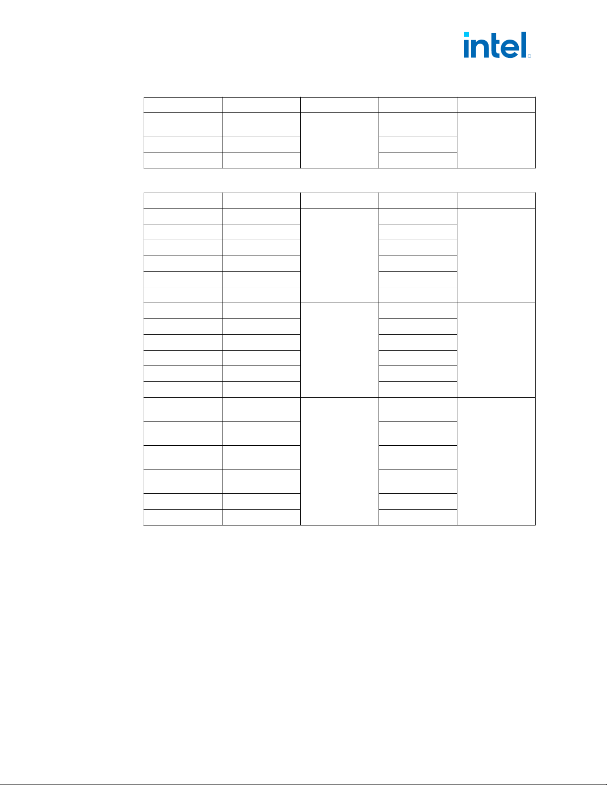
Table 68. PX CSI-2 Lane Allocation Table
Pin Name Option 1 CFG Option 2 CFG
CSI_C_DP[1] CSI_C_DP[1]
X2
CSI_C_DP[1]
X2
CSI_C_DN[1] CSI_C_DN[1] CSI_C_DN[1]
CSI_C_DP[0] CSI_C_DP[0] CSI_C_DP[0]
CSI_C_DN[0] CSI_C_DN[0] CSI_C_DN[0]
CSI_C_CLK_P CSI_C_CLK_P CSI_C_CLK_P
CSI_C_CLK_N CSI_C_CLK_N CSI_C_CLK_N
CSI_B_DP[1] CSI_B_DP[1]
X2
CSI_B_DP[1]
X4
CSI_B_DN[1] CSI_B_DN[1] CSI_B_DN[1]
CSI_B_DP[0] CSI_B_DP[0] CSI_B_DP[0]
CSI_B_DN[0] CSI_B_DN[0] CSI_B_DN[0]
CSI_B_CLK_P CSI_B_CLK_P CSI_B_CLK_P
CSI_B_CLK_N CSI_B_CLK_N CSI_B_CLK_N
CSI_A_DP[1] /
CSI_B_DP[2]
CSI_A_DP[1]
X2
CSI_B_DP[2]
X4
CSI_A_DN[1] /
CSI_B_DN[2]
CSI_A_DN[1] CSI_B_DN[2]
CSI_A_DP[0] /
CSI_B_DP[3]
CSI_A_DP[0] CSI_B_DP[3]
CSI_A_DN[0] /
CSI_B_DN[3]
CSI_A_DN[0] CSI_B_DN[3]
CSI_A_CLK_P CSI_A_CLK_P Not Used
CSI_A_CLK_N CSI_A_CLK_N Not Used
R
Camera/MIPI—Intel
®
Core
™
, Xeon
™
6300 And Xeon
™
E 2400 Processors
13
th
Generation Intel
®
Core
™
, Intel
®
Core
™
14
th
Generation, Intel
®
Core
™
Processor (Series 1) and (Series 2), Intel
®
Xeon
™
E
2400 Processor and Intel
®
Xeon
™
6300 Processor
May 2025 Datasheet, Volume 1 of 2
Doc. No.: 743844, Rev.: 015 167