743844-015.pdf - 第125页
Data Scrambling The system memory controller incorporates a Data Scr ambling feature to minimize the impact of excessive di/dt on the platform system memory VRs due to successive 1s and 0s on the data bus. Past experienc…
When both channels are populated with the same memory capacity and the boundary
between the dual channel zone and the single channel zone is the top of memory, IMC
operates completely in Dual-Channel Symmetric mode.
NOTES
• The DRAM device technology and width may vary from one channel to another.
• Different memory size between channels are relevant to DDR4 and DDR5 only.
System Memory Frequency
In all modes, the frequency of system memory is the lowest frequency and latency of
all memory modules placed in the system, as determined through the SPD registers
on the memory modules. The system memory controller supports a single DIMM
connector per channel. If DIMMs with different latency are populated across the
channels, the BIOS will use the slower of the two latencies for both channels. For
Dual-Channel modes, both channels should have a DIMM connector populated. For
Single-Channel mode, only a single channel can have a DIMM connector populated.
Technology Enhancements of Intel
®
FMA
The following sections describe the Just-in-Time Scheduling, Command Overlap, and
Out-of-Order Scheduling Intel
®
Fast Memory Access (Intel
®
FMA) technology
enhancements.
Just-in-Time Command Scheduling
The memory controller has an advanced command scheduler where all pending
requests are examined simultaneously to determine the most efficient request to be
issued next. The most efficient request is picked from all pending requests and issued
to system memory Just-in-Time to make optimal use of Command Overlapping. Thus,
instead of having all memory access requests go individually through an arbitration
mechanism forcing requests to be executed one at a time, they can be started without
interfering with the current request allowing for concurrent issuing of requests. This
allows for optimized bandwidth and reduced latency while maintaining appropriate
command spacing to meet system memory protocol.
Command Overlap
Command Overlap allows the insertion of the DRAM commands between the Activate,
Pre-charge, and Read/Write commands normally used, as long as the inserted
commands do not affect the currently executing command. Multiple commands can be
issued in an overlapping manner, increasing the efficiency of system memory protocol.
Out-of-Order Scheduling
While leveraging the Just-in-Time Scheduling and Command Overlap enhancements,
the IMC continuously monitors pending requests to system memory for the best use of
bandwidth and reduction of latency. If there are multiple requests to the same open
page, these requests would be launched in a back to back manner to make optimum
use of the open memory page. This ability to reorder requests on the fly allows the
IMC to further reduce latency and increase bandwidth efficiency.
5.1.7
5.1.8
R
Intel
®
Core
™
, Xeon
™
6300 And Xeon
™
E 2400 Processors—Memory
13
th
Generation Intel
®
Core
™
, Intel
®
Core
™
14
th
Generation, Intel
®
Core
™
Processor (Series 1) and (Series 2), Intel
®
Xeon
™
E
2400 Processor and Intel
®
Xeon
™
6300 Processor
Datasheet, Volume 1 of 2 May 2025
124 Doc. No.: 743844, Rev.: 015
Data Scrambling
The system memory controller incorporates a Data Scrambling feature to minimize the
impact of excessive di/dt on the platform system memory VRs due to successive 1s
and 0s on the data bus. Past experience has demonstrated that traffic on the data bus
is not random and can have energy concentrated at specific spectral harmonics
creating high di/dt which is generally limited by data patterns that excite resonance
between the package inductance and on die capacitances. As a result, the system
memory controller uses a data scrambling feature to create pseudo-random patterns
on the system memory data bus to reduce the impact of any excessive di/dt.
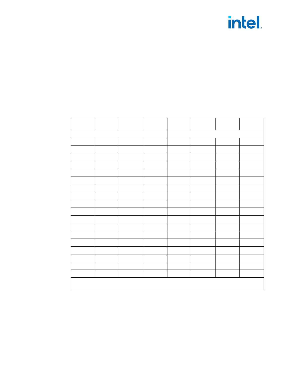
ECC H-Matrix Syndrome Codes
Syndrome
Value
Flipped
Bit
Syndrome
Value
Flipped
Bit
Syndrome
Value
Flipped
Bit
Syndrome
Value
Flipped
Bit
0 No Error
1 64 37 26 81 2 146 53
2 65 38 46 82 18 148 4
4 66 41 61 84 34 152 20
7 60 42 9 88 50 161 49
8 67 44 16 97 21 162 1
11 36 47 23 98 38 164 17
13 27 49 63 100 54 168 33
14 3 50 47 104 5 176 44
16 68 52 14 112 52 193 8
19 55 56 30 128 71 194 24
21 10 64 70 131 22 196 40
22 29 67 6 133 58 200 56
25 45 69 42 134 13 208 19
26 57 70 62 137 28 224 11
28 0 73 12 138 41 241 7
31 15 74 25 140 48 242 31
32 69 76 32 143 43 244 59
35 39 79 51 145 37 248 35
Notes: 1. All other syndrome values indicate unrecoverable error (more than one error).
2. This table is relevant only for S-Processor ECC supported SKUs.
Data Swapping
By default, the processor supports on-board data swapping in two manners (for all
segments and DRAM technologies):
• DQ swapping is allowed within each Byte for all DDR technologies.
•
• LPDDR4x byte cannot be swizzled within their x16 sub-channel
5.1.9
5.1.10
5.1.11
R
Memory—Intel
®
Core
™
, Xeon
™
6300 And Xeon
™
E 2400 Processors
13
th
Generation Intel
®
Core
™
, Intel
®
Core
™
14
th
Generation, Intel
®
Core
™
Processor (Series 1) and (Series 2), Intel
®
Xeon
™
E
2400 Processor and Intel
®
Xeon
™
6300 Processor
May 2025 Datasheet, Volume 1 of 2
Doc. No.: 743844, Rev.: 015 125
• LPDDR4x x16 sub-channels can be swizzled within their x32 channel
• LPDDR4x x32 channels can be swizzled within their x64 MC
• LPDDR5/x x16 sub-channels can be swizzle within their x64 MC
• DDR4: Byte swapping is allowed within each x64 Channel.
• DDR5: Byte swapping is allowed within a channel in 16-bit group: [0,1] [2,3 ].
• ECC bits swap is allowed within ECC byte/nibble: DDR4 ECC[7..0] and DDR5
ECC[3..0].
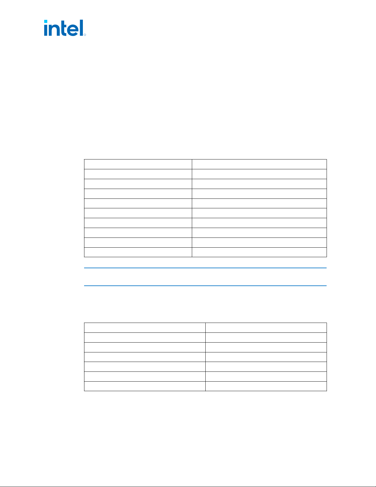
LPDDR5/x Ascending and Descending
LPDDR5/x support Ascending / descending that swap CA and CS signals connectivity
order.
Ascending Descending
CA6 CA0
CA5 CA1
CA4 CS_1
CA3 CS_0
CA2 CA2
CS_0 CA3
CS_1 CA4
CA1 CA5
CA0 CA6
NOTE
Ascending / descending can be performed in every x16 sub channel.
LPDDR4x CMD Mirroring
LPDDR4x support Mirroring that swap CA signals connectivity order.
Default Mirrored
CA 0 CA 5
CA 1 CA 4
CA 2 CA 3
CA 3 CA 2
CA 4 CA 1
CA 5 CA 0
5.1.12
5.1.13
R
Intel
®
Core
™
, Xeon
™
6300 And Xeon
™
E 2400 Processors—Memory
13
th
Generation Intel
®
Core
™
, Intel
®
Core
™
14
th
Generation, Intel
®
Core
™
Processor (Series 1) and (Series 2), Intel
®
Xeon
™
E
2400 Processor and Intel
®
Xeon
™
6300 Processor
Datasheet, Volume 1 of 2 May 2025
126 Doc. No.: 743844, Rev.: 015