743844-015.pdf - 第145页
PCI Express* Architecture Compatibility with the PCI addressing model is maintained to ensure that all existing applications and drivers operate unchanged. The PCI Express* configuration uses standard mechanisms as defin…
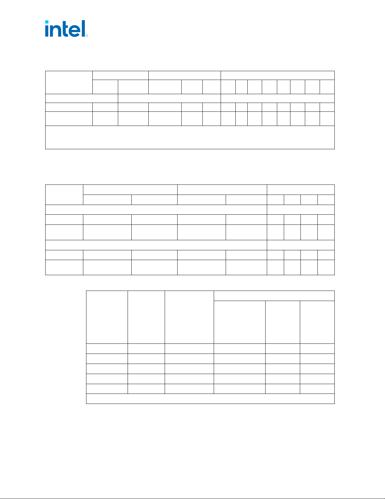
Table 53. H/H Refresh/PX PCI Express* 8 - Lane Reversal Mapping
Bifurcation
Link Width CFG Signals Lanes
0:1:0 0:1:1
CFG
[6]
CFG
[5]
CFG
[2]
0 1 2 3 4 5 6 7
PCIe controller PCIe 010 (PEG10)
1x8 x8 N/A 1 1 1 0 1 2 3 4 5 6 7
1x8
Reversed
x8 N/A 1 1 0 7 6 5 4 3 2 1 0
Notes: 1. For CFG bus details, refer to
Reset and Miscellaneous Signals on page 175.
2. Support is also provided for narrow width and use devices with lower number of lanes (that is, usage on x4 configuration), however further
bifurcation is not supported.
3. For reversal lanes, for example: When using 1x4, the 4 lane device should use lanes 4:7, so lane 7 will be connected to lane 0 of the Device.
The H/H Refresh/PX/P/U/U Refresh processor Lines supports the configurations shown
in the following tables:
Table 54. H/H Refresh/PX/P/U/U Refresh PCI Express* 4 - Lane Reversal Mapping
Bifurcation
Link Width CFG Signals Lanes
0:6:0 0:6:2 CFG [14] CFG [15] 0 1 2 3
PCIe Controller PCIe 060 (PEG60)
1x4 x4 NA 1 NA 0 1 2 3
1x4
Reversed
x4 NA 0 NA 3 2 1 0
PCIe Controller PCIe 062 (PEG62)
1x4 NA x4 NA 1 0 1 2 3
1x4
Reversed
NA x4 NA 0 3 2 1 0
Table 55. PCI Express* Maximum Transfer Rates and Theoretical Bandwidth
PCI Express*
Generation
Encoding
Maximum
Transfer Rate
[GT/s]
Theoretical Bandwidth [GB/s]
S/S
Refresh/E/H/H
Refresh/HX/HX
Refresh /P/U/U
Refresh
x4
S/S
Refresh/E/
H/H
Refresh/H
X/HX
Refresh
x8
S/S
Refresh/E/
HX/HX
Refresh
x16
Gen 1 8b/10b 2.5 1.0 2.0 4.0
Gen 2 8b/10b 5 2.0 4.0 8.0
Gen 3 128b/130b 8 3.9 7.9 15.8
Gen 4 128b/130b 16 7.9 15.8 31.5
Gen 5 128b/130b 32
1
15.8
1
31.5
1
63
1
Note: 1. Transfer rate and max theoretical Bandwidth are not final and could be lowered.
The above table summarizes the transfer rates and theoretical bandwidth of PCI
Express* link.
R
Intel
®
Core
™
, Xeon
™
6300 And Xeon
™
E 2400 Processors—PCIe* Interface
13
th
Generation Intel
®
Core
™
, Intel
®
Core
™
14
th
Generation, Intel
®
Core
™
Processor (Series 1) and (Series 2), Intel
®
Xeon
™
E
2400 Processor and Intel
®
Xeon
™
6300 Processor
Datasheet, Volume 1 of 2 May 2025
144 Doc. No.: 743844, Rev.: 015
PCI Express* Architecture
Compatibility with the PCI addressing model is maintained to ensure that all existing
applications and drivers operate unchanged.
The PCI Express* configuration uses standard mechanisms as defined in the PCI Plug-
and-Play specification.
The processor PCI Express* port supports Gen 4 at 16GT/s uses a 128b/130b
encoding and Gen 5 at 32 GT/s uses a 128b/130b encoding
S/HX/S Refresh/HX Refresh/E/E Refresh-Processor Line: The 4 lanes port can
operate at 2.5 GT/s, 5 GT/s, 8 GT/s or 16 GT/s.
S/HX/S Refresh/HX Refresh/E/E Refresh-Processor Line: The 16 lanes port
can operate at 2.5 GT/s, 5 GT/s, 8 GT/s, 16 GT/s or 32 GT/s**
H/H Refresh/P/PX/U/U Refresh -Processor Line: Each of the 4 lanes ports can
operate at 2.5 GT/s, 5 GT/s, 8 GT/s or 16 GT/s.
H/H Refresh-Processor Line: The 8 lane port can operate at 2.5 GT/s, 5 GT/s, 8
GT/s, 16 GT/s or 32 GT/s**
PX-Processor Line: The 8 lane port can operate at 2.5 GT/s, 5 GT/s, 8 GT/s, or 16
GT/s**
The PCI Express* architecture is specified in three layers – Transaction Layer, Data
Link Layer, and Physical Layer. Refer to the PCI Express Base Specification 5.0 for
details of PCI Express* architecture.
PCI Express* Configuration Mechanism
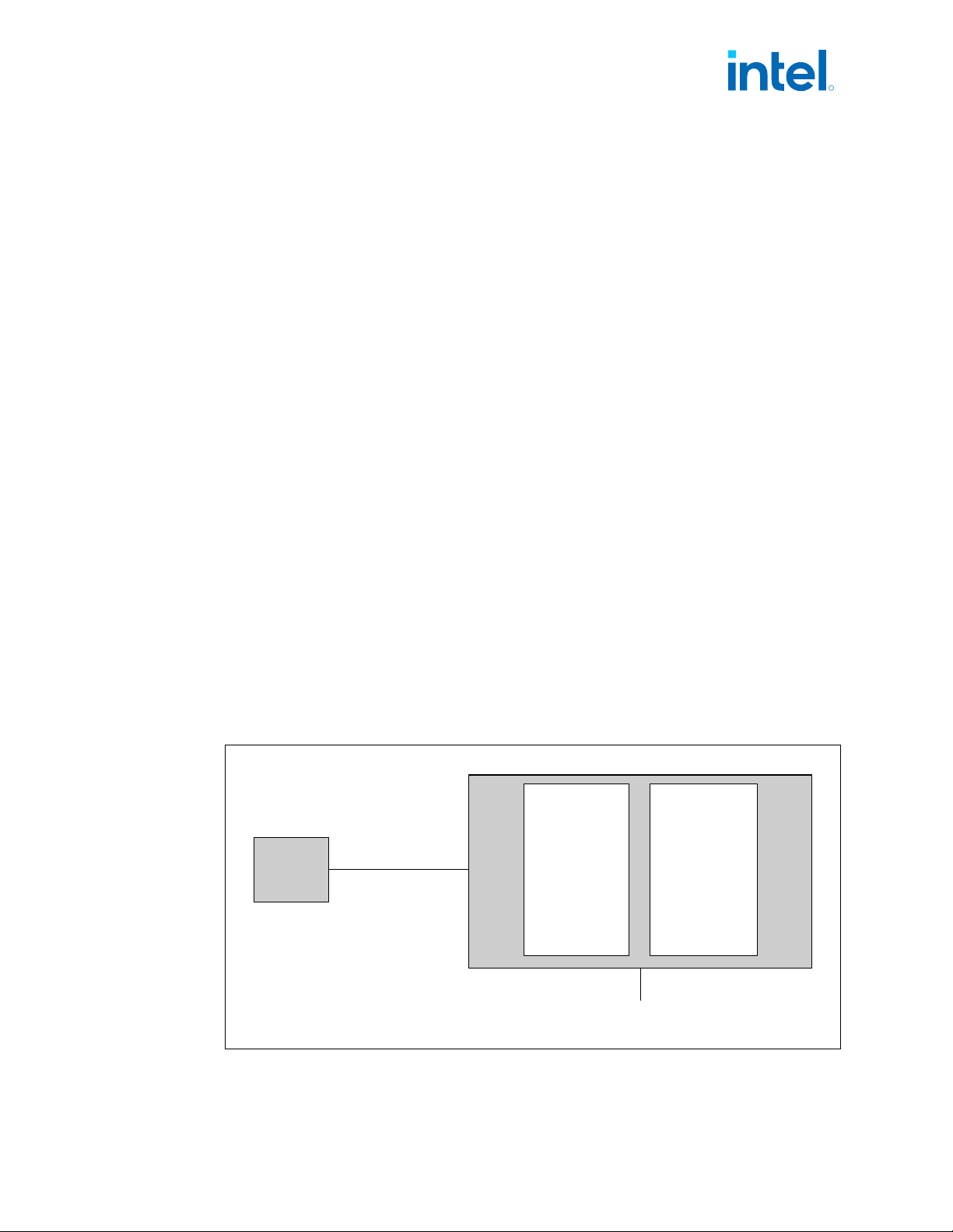
The PCI Express* (external graphics) link is mapped through a PCI-to-PCI bridge
structure.
Figure 21. PCI Express* Related Register Structures in the Processor
PCI-PCI Bridge
representing
root PCI
Express* ports
(Device 1)
PCI Compatible
Host Bridge
Device
(Device 0)
PCI
Express*
Device
PEG
DMI
7.1.2
7.1.3
R
PCIe* Interface—Intel
®
Core
™
, Xeon
™
6300 And Xeon
™
E 2400 Processors
13
th
Generation Intel
®
Core
™
, Intel
®
Core
™
14
th
Generation, Intel
®
Core
™
Processor (Series 1) and (Series 2), Intel
®
Xeon
™
E
2400 Processor and Intel
®
Xeon
™
6300 Processor
May 2025 Datasheet, Volume 1 of 2
Doc. No.: 743844, Rev.: 015 145

The PCI Express* Host Bridge is required to translate the memory-mapped PCI
Express* configuration space accesses from the host processor to PCI Express*
configuration cycles. To maintain compatibility with PCI configuration addressing
mechanisms, it is recommended that system software access the enhanced
configuration space using 32-bit operations (32-bit aligned) only. Refer to the PCI
Express Base Specification for details of both the PCI-compatible and PCI Express*
Enhanced configuration mechanisms and transaction rules.
PCI Express* Equalization Methodology
Link equalization requires equalization for both TX and RX sides for the processor and
for the Endpoint device.
Adjusting transmitter and receiver of the lanes is done to improve signal reception
quality and for improving link robustness and electrical margin.
The link timing margins and voltage margins are strongly dependent on equalization of
the link.
The processor supports the following:
• Full TX Equalization: Three Taps Linear Equalization (Pre, Current and Post
cursors), with FS/LF (Full Swing /Low Frequency) values.
• Full RX Equalization and acquisition for AGC (Adaptive Gain Control), CDR (Clock
and Data Recovery), adaptive DFE (decision feedback equalizer) and adaptive
CTLE peaking (continuous time linear equalizer).
• Full adaptive phase 3 EQ compliant with PCI Express* Gen 3 and Gen 4
specification.
PCI Express* Hot Plug
PCI Express Hot Plug not supported.
7.1.4
7.1.5
R
Intel
®
Core
™
, Xeon
™
6300 And Xeon
™
E 2400 Processors—PCIe* Interface
13
th
Generation Intel
®
Core
™
, Intel
®
Core
™
14
th
Generation, Intel
®
Core
™
Processor (Series 1) and (Series 2), Intel
®
Xeon
™
E
2400 Processor and Intel
®
Xeon
™
6300 Processor
Datasheet, Volume 1 of 2 May 2025
146 Doc. No.: 743844, Rev.: 015