743844-015.pdf - 第170页
Signal Name Description Dir. Buffer Type Link Type Availability DDR0_ACT# DDR1_ACT# Activation Command: ACT# HIGH along with CS_N determines that the signals addresses below have command functionality . O DDR4 SE S/S Ref…
System Memory Interface
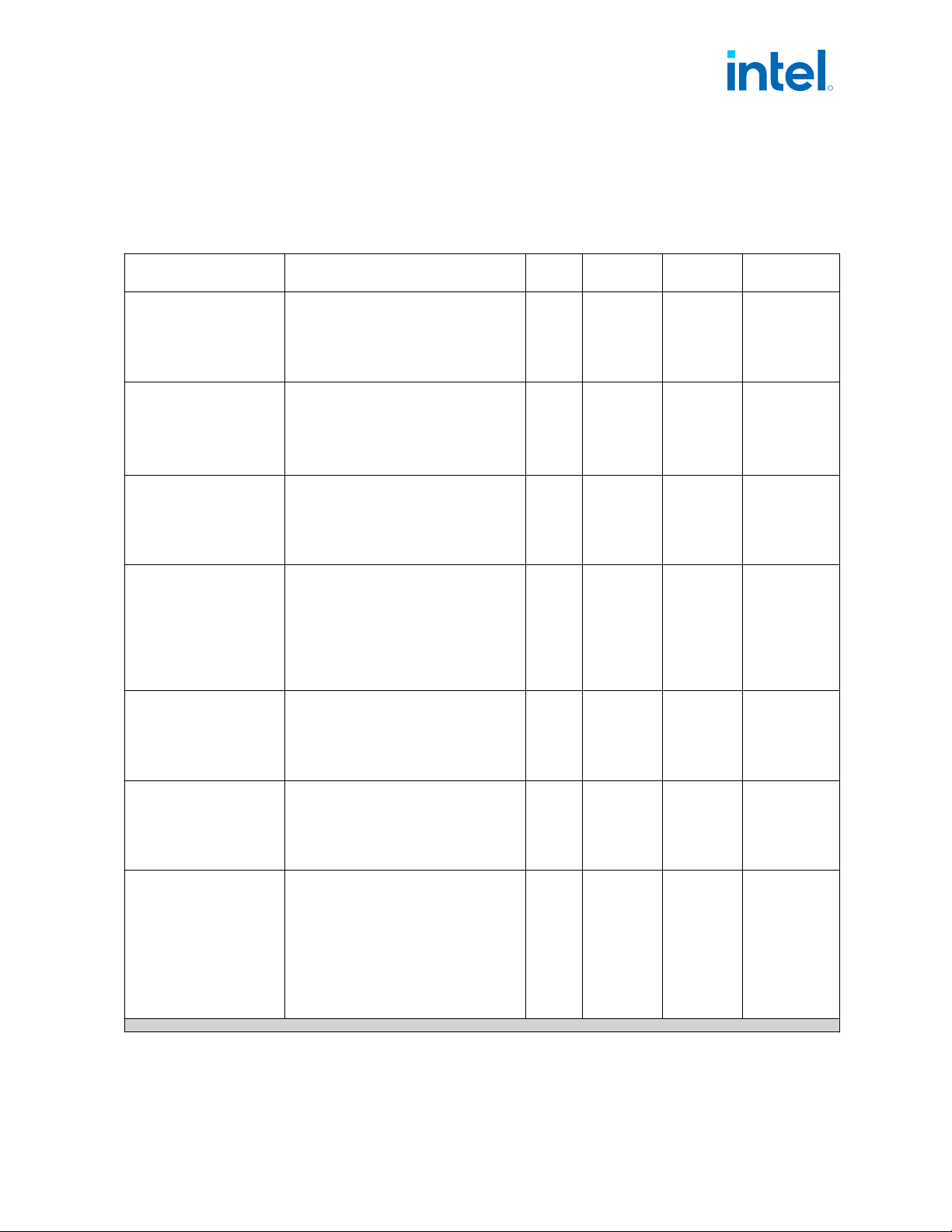
DDR4 Memory Interface
Table 70. DDR4 Memory Interface
Signal Name Description Dir.
Buffer
Type
Link Type Availability
DDR0_DQ[8:0][[7:0]]
DDR1_DQ[8:0][[7:0]]
Data Buses: Data signals interface to
the SDRAM data buses.
Example: DDR0_DQ2[5] refers to DDR
channel 0, Byte 2, Bit 5.
I/O DDR4 SE
S/S
Refresh/H/P/P
X/HX/HX
Refresh/U/U
Refresh
Processor Line
DDR0_DQSP[8:0]
DDR1_DQSP[8:0]
DDR0_DQSN[8:0]
DDR1_DQSN[8:0]
Data Strobes: Differential data strobe
pairs. The data is captured at the
crossing point of DQS during reading and
write transactions.
Example: DDR0_DQSP0 refers to DQSP
of DDR channel 0, Byte 0.
I/O DDR4 Diff
S/S
Refresh/H/P/P
X/HX/HX
Refresh/U/U
Refresh
Processor Line
DDR0_CLKN[3:0]
DDR0_CLKP[3:0]
DDR1_CLKN[3:0]
DDR1_CLKP[3:0]
SDRAM Differential Clock: Differential
clocks signal pairs, pair per rank. The
crossing of the positive edge and the
negative edge of their complement are
used to sample the command and
control signals on the SDRAM.
O DDR4 Diff
S/S
Refresh/H/P/P
X/HX/HX
Refresh/U/U
Refresh
Processor Line
DDR0_CKE[3:0]
DDR1_CKE[3:0]
Clock Enable: (1 per rank). These
signals are used to:
• Initialize the SDRAMs during power-
up.
• Power-down SDRAM ranks.
• Place all SDRAM ranks into and out of
self-refresh during STR (Suspend to
RAM).
O DDR4 SE
S/S
Refresh/H/P/P
X/HX/HX
Refresh/U/U
Refresh
Processor Line
DDR0_CS[3:0]
DDR1_CS[3:0]
Chip Select: (1 per rank). These signals
are used to select particular SDRAM
components during the active state.
There is one Chip Select for each SDRAM
rank.
O DDR4 SE
S/S
Refresh/H/P/P
X/HX/HX
Refresh/U/U
Refresh
Processor Line
DDR0_ODT[3:0]
DDR1_ODT[3:0]
On Die Termination: (1 per rank).
Active SDRAM Termination Control.
O DDR4 SE
S/S
Refresh/H/P/P
X/HX/HX
Refresh/U/U
Refresh
Processor Line
DDR0_MA[16:0]
DDR1_MA[16:0]
Address: These signals are used to
provide the multiplexed row and column
address to the SDRAM.
DDR0_MA[16] uses as RAS# signal
DDR0_MA[15] uses as CAS# signal
DDR0_MA[14] uses as WE# signal
DDR1_MA[16] uses as RAS# signal
DDR1_MA[15] uses as CAS# signal
DDR1_MA[14] uses as WE# signal
O DDR4 SE
S/S
Refresh/H/P/P
X/HX/HX
Refresh/U/U
Refresh
Processor Line
continued...
12.1
12.1.1
R
Signal Description—Intel
®
Core
™
, Xeon
™
6300 And Xeon
™
E 2400 Processors
13
th
Generation Intel
®
Core
™
, Intel
®
Core
™
14
th
Generation, Intel
®
Core
™
Processor (Series 1) and (Series 2), Intel
®
Xeon
™
E
2400 Processor and Intel
®
Xeon
™
6300 Processor
May 2025 Datasheet, Volume 1 of 2
Doc. No.: 743844, Rev.: 015 169
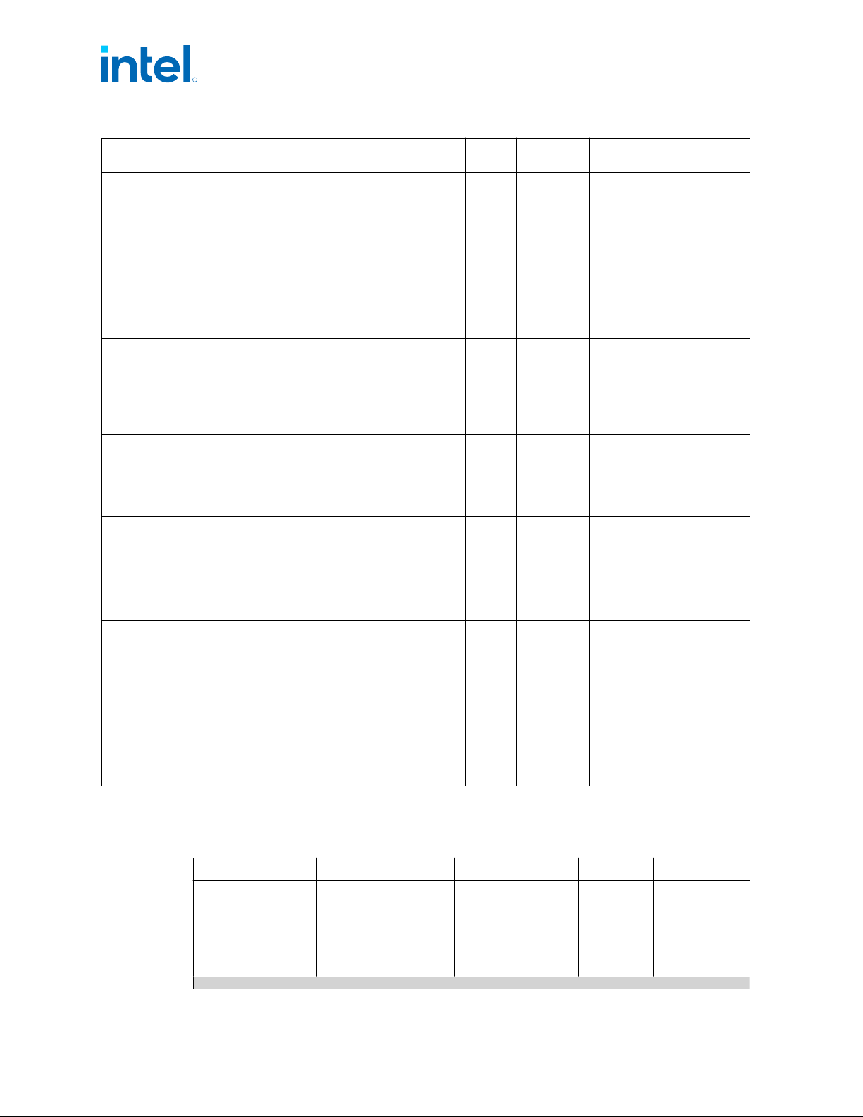
Signal Name Description Dir.
Buffer
Type
Link Type Availability
DDR0_ACT#
DDR1_ACT#
Activation Command: ACT# HIGH
along with CS_N determines that the
signals addresses below have command
functionality.
O DDR4 SE
S/S
Refresh/H/P/P
X/HX/HX
Refresh/U/U
Refresh
Processor Line
DDR0_BG[1:0]
DDR1_BG[1:0]
Bank Group: BG[1:0] define to which
bank group an Active, reading, Write or
Precharge command is being applied.
BG0 also determines which mode
register is to be accessed during a MRS
cycle.
O DDR4 SE
S/S
Refresh/H/P/P
X/HX/HX
Refresh/U/U
Refresh
Processor Line
DDR0_BA[1:0]
DDR1_BA[1:0]
Bank Address: BA[1:0] define to which
bank an Active, reading, Write or
Precharge command is being applied.
Bank address also determines which
mode
register is to be accessed during a MRS
cycle.
O DDR4 SE
S/S
Refresh/H/P/P
X/HX/U
Processor Line
DDR0_PAR
DDR1_PAR
Command and Address Parity: These
signals are used for parity check.
O A SE
S/S
Refresh/H/P/P
X/HX/HX
Refresh/U/U
Refresh
Processor Line
DDR_VREF_CA[3:0]
Memory Reference Voltage for
Command and Address
O A SE
S/S
Refresh/HX/HX
Refresh
Processor Line
DDR0_VREF_CA0
DDR1_VREF_CA0
Memory Reference Voltage for
Command and Address
O A SE
H/P/U/U
Refresh
Processor Line
DDR_VTT_CTL
System Memory Power Gate Control:
When signal is high – platform memory
VTT regulator is enable, output high.
When signal is low - Disables the
platform memory VTT regulator in C8
and deeper and S3.
O A SE
S/S
Refresh/H/P/P
X/HX/HX
Refresh/U/U
Refresh
Processor Line
DDR0_ALERT#
DDR1_ALERT#
Alert: This signal is used at command
training only. It is getting the Command
and Address Parity error flag during
training. CRC feature is not supported.
I DDR4 SE
S/S
Refresh/H/P/P
X/HX/HX
Refresh/U/U
Refresh
Processor Line
LP4x-LP5 Memory Interface
Table 71. LP4x-LP5 Memory Interface
Signal Name Description Dir. Buffer Type Link Type Availability
DDR0_DQ[1:0][7:0]
DDR1_DQ[1:0][7:0]
DDR2_DQ[1:0][7:0]
DDR3_DQ[1:0][7:0]
DDR4_DQ[1:0][7:0]
DDR5_DQ[1:0][7:0]
Data Buses: Data
signals interface to the
SDRAM data buses.
Example:
DDR0_DQ1[5] refers to
DDR channel 0, Byte 1,
Bit 5.
I/O LP4x-LP5 SE P/H/PX/HX/HX
Refresh/U/U
Refresh
Processor Line
continued...
12.1.2
R
Intel
®
Core
™
, Xeon
™
6300 And Xeon
™
E 2400 Processors—Signal Description
13
th
Generation Intel
®
Core
™
, Intel
®
Core
™
14
th
Generation, Intel
®
Core
™
Processor (Series 1) and (Series 2), Intel
®
Xeon
™
E
2400 Processor and Intel
®
Xeon
™
6300 Processor
Datasheet, Volume 1 of 2 May 2025
170 Doc. No.: 743844, Rev.: 015
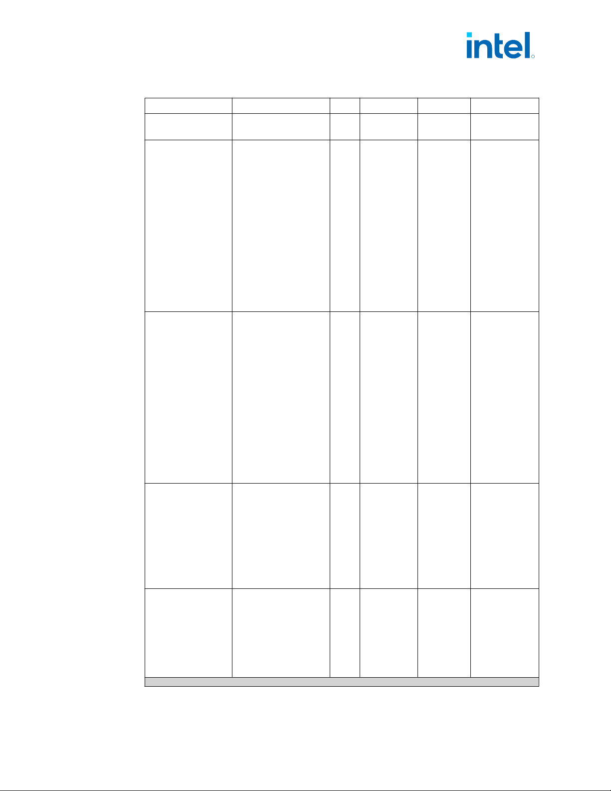
Signal Name Description Dir. Buffer Type Link Type Availability
DDR6_DQ[1:0][7:0]
DDR7_DQ[1:0][7:0]
DDR0_DQSP[1:0]
DDR1_DQSP[1:0]
DDR2_DQSP[1:0]
DDR3_DQSP[1:0]
DDR4_DQSP[1:0]
DDR5_DQSP[1:0]
DDR6_DQSP[1:0]
DDR7_DQSP[1:0]
DDR0_DQSN[1:0]
DDR1_DQSN[1:0]
DDR2_DQSN[1:0]
DDR3_DQSN[1:0]
DDR4_DQSN[1:0]
DDR5_DQSN[1:0]
DDR6_DQSN[1:0]
DDR7_DQSN[1:0]
Data Strobes:
Differential data strobe
pairs. The data is
captured at the crossing
point of DQS during
reading and write
transactions.
I/O LP4x-LP5 Diff P/H/PX/HX/HX
Refresh/U/U
Refresh
Processor Line
DDR0_CLK_N
DDR0_CLK_P
DDR1_CLK_N
DDR1_CLK_P
DDR2_CLK_N
DDR2_CLK_P
DDR3_CLK_N
DDR3_CLK_P
DDR4_CLK_N
DDR4_CLK_P
DDR5_CLK_N
DDR5_CLK_P
DDR6_CLK_N
DDR6_CLK_P
DDR7_CLK_N
DDR7_CLK_P
SDRAM Differential
Clock:
Differential clocks signal
pairs, pair per channel
and package. The
crossing of the positive
edge and the negative
edge of their
complement are used to
sample the command
and control signals on
the SDRAM.
O LP4x-LP5 Diff P/H/PX/HX/HX
Refresh/U/U
Refresh
Processor Line
DDR0_CKE[1:0]
DDR1_CKE[1:0]
DDR2_CKE[1:0]
DDR3_CKE[1:0]
DDR4_CKE[1:0]
DDR5_CKE[1:0]
DDR6_CKE[1:0]
DDR7_CKE[1:0]
Clock Enable: (1 per
rank) These signals are
used to:
• Initialize the SDRAMs
during power-up.
• Power-down SDRAM
ranks.
• Place all SDRAM
ranks into and out of
self-refresh during
STR.
O LP4x-LP5 SE P/H/PX/HX/HX
Refresh/U/U
Refresh /U
RefreshProcesso
r Line
DDR0_CS[1:0]
DDR1_CS[1:0]
DDR2_CS[1:0]
DDR3_CS[1:0]
DDR4_CS[1:0]
DDR5_CS[1:0]
DDR6_CS[1:0]
DDR7_CS[1:0]
Chip Select: (1 per
rank). These signals are
used to select particular
SDRAM components
during the active state.
There is one Chip Select
for each SDRAM rank.
The Chip select signal is
Active High.
O LP4x-LP5 SE P/H/PX/HX/HX
Refresh/U/U
Refresh
Processor Line
continued...
R
Signal Description—Intel
®
Core
™
, Xeon
™
6300 And Xeon
™
E 2400 Processors
13
th
Generation Intel
®
Core
™
, Intel
®
Core
™
14
th
Generation, Intel
®
Core
™
Processor (Series 1) and (Series 2), Intel
®
Xeon
™
E
2400 Processor and Intel
®
Xeon
™
6300 Processor
May 2025 Datasheet, Volume 1 of 2
Doc. No.: 743844, Rev.: 015 171