743844-015.pdf - 第174页
PCI Express* Graphics (PEG) Signals Signal Name Description Dir Buffer Type Link Type Availability PCIE_X4_TXP[[3:0]] PCIE_X4_TXN[[3:0]] PCIe T ransmit Differential P airs O PCIE* Diff S/S Refresh/E/E Refresh /HX/HX R ef…
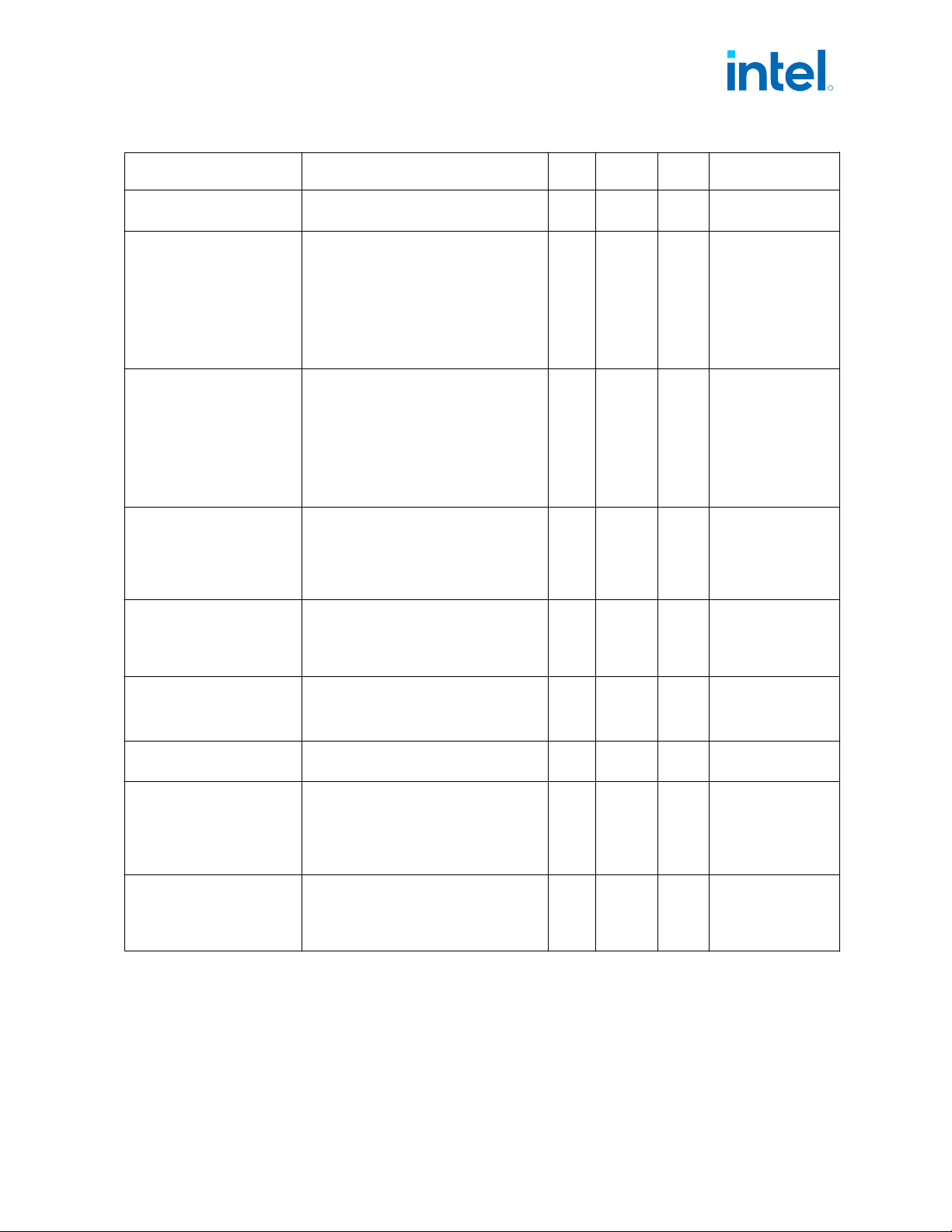
Signal Name Description Dir.
Buffer
Type
Link
Type
Availability
DDR3_DQ3[7:0]
DDR3_DQ4[3:0]
DDR0_DQSP[4:0]
DDR0_DQSN[4:0]
DDR1_DQSP[4:0]
DDR1_DQSN[4:0]
DDR2_DQSP[4:0]
DDR2_DQSN[4:0]
DDR3_DQSP[4:0]
DDR3_DQSN[4:0]
Data Strobes: Differential data strobe
pairs. The data is captured at the crossing
point of DQS during reading and write
transactions.
Example: DDR0_DQSP0 refers to DQSP
of DDR channel 0, Byte 0.
I/O DDR5 Diff
S/S Refresh/E/E
Refresh
H/P/PX/HX/HX
Refresh/U/U Refresh
Processor Line
DDR0_CLKN[3:0]
DDR0_CLKP[3:0]
DDR1_CLKN[3:0]
DDR1_CLKP[3:0]
DDR2_CLKN[3:0]
DDR2_CLKP[3:0]
DDR3_CLKN[3:0]
DDR3_CLKP[3:0]
SDRAM Differential Clock: Differential
clocks signal pairs, pair per rank. The
crossing of the positive edge and the
negative edge of their complement are
used to sample the command and control
signals on the SDRAM.
O DDR5 Diff
S/S Refresh/E/E
Refresh
H/P/PX/HX/HX
Refresh/U/U Refresh
Processor Line
DDR0_CS[3:0]
DDR1_CS[3:0]
DDR2_CS[3:0]
DDR3_CS[3:0]
Chip Select: (1 per rank). These signals
are used to select particular SDRAM
components during the active state.
There is one Chip Select for each SDRAM
rank.
The Chip select signal is Active Low.
O DDR5 SE
S/S Refresh/E/E
Refresh
H/P/PX/HX/HX
Refresh/U/U Refresh
Processor Line
DDR0_CA[12:0]
DDR1_CA[12:0]
DDR2_CA[12:0]
DDR3_CA[12:0]
Command Address: These signals are
used to provide the multiplexed command
and address to the SDRAM.
O DDR5 SE
S/S Refresh/E/E
Refresh /P/PX/HX/H
X Refresh/U/U
Refresh Processor
Line
DDR_VREF_CA[3:0]
Memory Reference Voltage for
Command and Address
O A SE
S/S Refresh/E/E
Refresh /HX/HX
Refresh Processor
Line
DDR0_VREF_CA0
DDR1_VREF_CA0
Memory Reference Voltage for
Command and Address
O A SE
H/P/U/U Refresh
Processor Line
DDR_VTT_CTL
System Memory Power Gate Control:
When signal is high – platform memory
VTT regulator is enable, output high.
When signal is low - Disables the platform
memory VTT regulator in C8 and deeper
and S3.
O A SE
S/S Refresh/E/E
Refresh
H/P/PX/HX/HX
Refresh/U/U Refresh
Processor Line
DDR0_ALERT#
DDR1_ALERT#
Alert: This signal is used at command
training only. It is getting the Command
and Address Parity error flag during
training. CRC feature is not supported.
I DDR5 SE
S/S Refresh/E/E
Refresh
H/P/PX/HX/HX
Refresh/U/U Refresh
Processor Line
R
Signal Description—Intel
®
Core
™
, Xeon
™
6300 And Xeon
™
E 2400 Processors
13
th
Generation Intel
®
Core
™
, Intel
®
Core
™
14
th
Generation, Intel
®
Core
™
Processor (Series 1) and (Series 2), Intel
®
Xeon
™
E
2400 Processor and Intel
®
Xeon
™
6300 Processor
May 2025 Datasheet, Volume 1 of 2
Doc. No.: 743844, Rev.: 015 173
PCI Express* Graphics (PEG) Signals
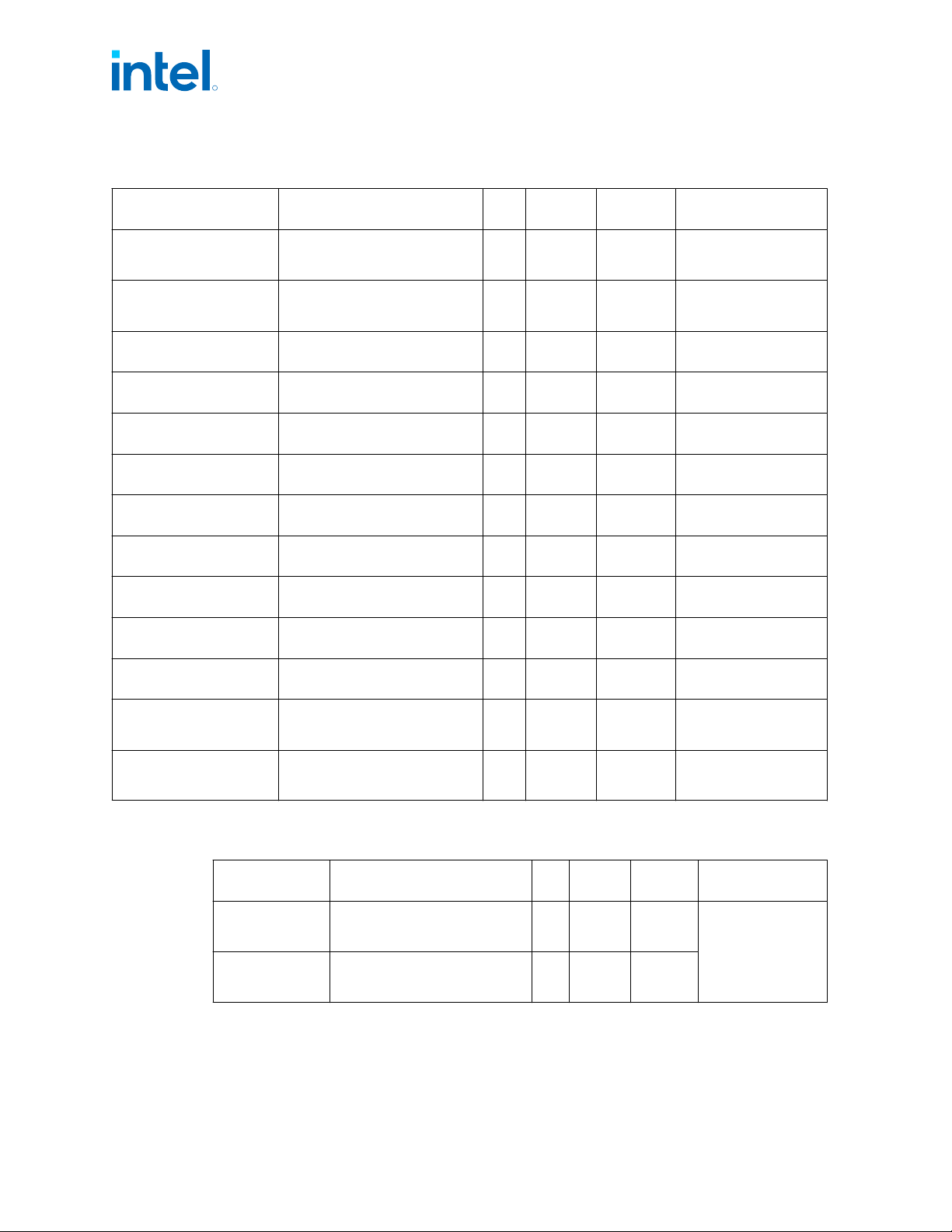
Signal Name Description Dir
Buffer
Type
Link
Type
Availability
PCIE_X4_TXP[[3:0]]
PCIE_X4_TXN[[3:0]]
PCIe Transmit Differential Pairs
O PCIE* Diff
S/S Refresh/E/E
Refresh /HX/HX Refresh
Processor Line
PCIE_X4_RXP[[3:0]]
PCIE_X4_RXN[[3:0]]
PCIe Receive Differential Pairs
I PCIE* Diff
S/S Refresh/E/E
Refresh /HX/HX Refresh
Processor Line
PCIEX4_A_TX_P[[3:0]]
PCIEX4_A_TX_N[[3:0]]
PCIe Transmit Differential Pairs
O PCIE* Diff
H/H Refresh/PX/P
Processor Line
PCIEX4_A_RX_P[[3:0]]
PCIEX4_A_RX_N[[3:0]]
PCIe Transmit Differential Pairs
I PCIE* Diff
H/H Refresh/PX/P
Processor Line
PCIEX4_A_RCOMP_P
PCIEX4_A_RCOMP_N
PCIe RCOMP Differential Pairs
NA A Diff
H/H Refresh/PX/P
Processor Line
PCIEX4_B_TXP[[3:0]]
PCIEX4_B_TXN[[3:0]]
PCIe Transmit Differential Pairs
O PCIE* Diff
H/H Refresh/P Processor
Line
PCIEX4_B_RXP[[3:0]]
PCIEX4_B_RXN[[3:0]]
PCIe Transmit Differential Pairs
I PCIE* Diff
H/H Refresh/P Processor
Line
PCIEX4_B_RCOMP_P
PCIEX4_B_RCOMP_N
PCIe RCOMP Differential Pairs
NA A Diff
H/H Refresh/P Processor
Line
PCIEX8_TX_P[[7:0]]
PCIEX8_TX_N[[7:0]]
PCIe Transmit Differential Pairs
O PCIE* Diff
H/H Refresh/PX
Processor Line
PCIEX8_RX_P[[7:0]]
PCIEX8_RX_N[[7:0]]
PCIe Transmit Differential Pairs
I PCIE* Diff
H/H Refresh/PX
Processor Line
PCIEX8_RCOMP_P
PCIEX8_RCOMP_N
PCIe RCOMP Differential Pairs
NA A Diff
H/H Refresh/PX
Processor Line
PCIE_X16_TXP[[15:0]]
PCIE_X16_TXN[[15:0]]
PCIe Transmit Differential Pairs
O PCIE* Diff
S/S Refresh/E/E
Refresh /HX/HX Refresh
Processor Line
PCIE_X16_RXP[[15:0]]
PCIE_X16_RXN[[15:0]]
PCIe Receive Differential Pairs
I PCIE* Diff
S/S Refresh/E/E
Refresh /HX/HX Refresh
Processor Line
Direct Media Interface (DMI) Signals
Signal Name Description Dir
Buffer
Type
Link
Type
Availability
DMI_RXP[7:0]
DMI_RXN[7:0]
DMI Input from PCH: Direct
Media Interface receive
differential pairs.
I DMI Diff
S/S Refresh/E/E
Refresh /HX/HX
Refresh-Processor
Line
DMI_TXP[7:0]
DMI_TXN[7:0]
DMI Output from PCH: Direct
Media Interface transmit
differential pairs.
O DMI Diff
12.2
12.3
R
Intel
®
Core
™
, Xeon
™
6300 And Xeon
™
E 2400 Processors—Signal Description
13
th
Generation Intel
®
Core
™
, Intel
®
Core
™
14
th
Generation, Intel
®
Core
™
Processor (Series 1) and (Series 2), Intel
®
Xeon
™
E
2400 Processor and Intel
®
Xeon
™
6300 Processor
Datasheet, Volume 1 of 2 May 2025
174 Doc. No.: 743844, Rev.: 015
Reset and Miscellaneous Signals
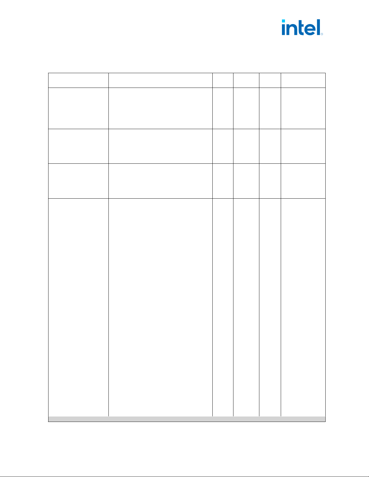
Signal Name Description Dir.
Buffer
Type
Link
Type
Availability
EKEY
Socket Electronic Key
Used to distinguish between packages with
different pins assignment. Connect this pin to
the Enable signal of the first VR in sequence.
Or as appropriate, to shut down complete
power to SOC/platform when a wrong
package is being used.
NA NA SE
S/S Refresh/E/E
Refresh , HX/HX
Refresh -
Processor Line
SKTOCC#
Socket Occupied: Pulled down directly (0
Ohms) on the processor package to the
ground. There is no connection to the
processor silicon for this signal. System board
designers may use this signal to determine if
the processor is present.
N/A N/A SE
P, H/H Refresh,
HX/HX Refresh,
PX, U/U Refresh -
Processor Line
SKTOCC#
Socket Occupied: Pulled down directly (0
Ohms) on the processor package to the
ground. There is no connection to the
processor silicon for this signal. System board
designers may use this signal to determine if
the processor is present.
O O SE
S/S Refresh/E/E
Refresh -
Processor Line
CFG[17:0]
Configuration Signals: The CFG signals have a
default value of '1' if not terminated on the
board.
Intel recommends placing test points on the
board for CFG pins.
• CFG[1:0]: Reserved configuration lane
• CFG[2]: S/S Refresh/E/E
Refresh /HX/HX Refresh - Processor
Line
PCI Express* Static X16 Lane Reversal
— 1 - Normal (default)
— 0 - Reversed
• CFG[2]: H/H Refresh/PX - Processor
Line
PCI Express* Static X16 Lane Reversal
— 1 - Normal (default)
— 0 - Reversed
• CFG[2] P/U/U Refresh-Processor Line
Reserved
• CFG[3]:
Reserved configuration lane.
• CFG[4]:
Reserved
• CFG[5] S/S Refresh/E/E
Refresh /HX/HX Refresh-Processor
Line
PCI Express* Bifurcation
— 0 = 2 x8 PCI Express*
— 1 = 1 x16 PCI Express* (default)
• CFG[5] H/H Refresh/P/PX/U/U
Refresh-Processor Line
Reserved
• CFG[6]:
Reserved configuration lanes.
• CFG[7]:
Reserved configuration lanes.
I/O GTL SE
S/S Refresh/E/E
Refresh -
Processor Line
P Processor Line
H/H Refresh
Processor Line
U/U Refresh
Processor Line
HX/HX Refresh-
Processor Line
PX-Processor Line
continued...
12.4
R
Signal Description—Intel
®
Core
™
, Xeon
™
6300 And Xeon
™
E 2400 Processors
13
th
Generation Intel
®
Core
™
, Intel
®
Core
™
14
th
Generation, Intel
®
Core
™
Processor (Series 1) and (Series 2), Intel
®
Xeon
™
E
2400 Processor and Intel
®
Xeon
™
6300 Processor
May 2025 Datasheet, Volume 1 of 2
Doc. No.: 743844, Rev.: 015 175