IPC-A-600H-2010 中文版 印制板的可接受性 (1).pdf - 第102页
‘‘A’’ Point of Narrowest Conductor Width: This is not ‘‘Minimum Conductor Width’’ noted on procurement documentation or perfor- mance specifications. ‘‘B’’ Conductor Base Width: The width that is measured when ‘‘Minimum …

Definitions used in evaluating etched conditions (see IPC-T-50) include:
评价蚀刻状况时所用到的定义(见IPC-T-50)包括:
Outgrowth: The increase in conductor width at one side of the conductor, caused by plating buildup over that delineated by the production
master.
镀层增宽: 由于镀层堆积引起的导体一侧宽度增加,超过生产底版的绘制宽度。
Undercut: The distance on one edge of the conductor measured parallel to the printed board surface from the outer edge of the conductor,
including etch resists, to the maximum point indentation to the copper conductor.
侧蚀: 从导体一侧外边缘(包括抗蚀层)到同一侧铜导体的最大凹入点与板面平行的间隔距离。
Overhang: The sum of the outgrowth and undercut.
镀层突沿: 镀层增宽和侧蚀量的总和。
Design width of conductor: The width of a conductor as delineated or noted on the procurement documentation.
Notes: 1. The ‘‘Production Master’’ may be adjusted for process methods and the artwork conductor width may differ from the design
width.
2. Design width of conductor is most often stated as a minimum as measured at the base of the conductor. For impedance controlled
circuits, a ± tolerance may be placed on conductor width.
导体设计宽度: 采购文件上绘制的或标注的导体宽度。
注:1. “生产底版”可以按加工方法进行调整,而照相底版的导体宽度可以不同于导体设计宽度。
2. 导体设计宽度通常是指在导体底部测量所得的最小宽度。对于阻抗可控的线路,其导体宽度可设置正负公差要求。
Production Master: A 1:1 scale pattern which is used to produce one or more printed boards within the accuracy specified on the procure-
ment documentation.
⽣产底版: 用于生产一块或多块印制板的按1:1比例绘制的图形,精度在采购文件规定的范围以内。
Etch Factor: The ratio of the depth of etch to the amount of lateral etch.
蚀刻系数: 蚀刻深度与侧向蚀刻量之比。
3.2 CONDUCTIVE PATTERNS – GENERAL(导电图形 – 总则)
Introduction(引⾔)
93IPC-A-600H-2010 2010年4月
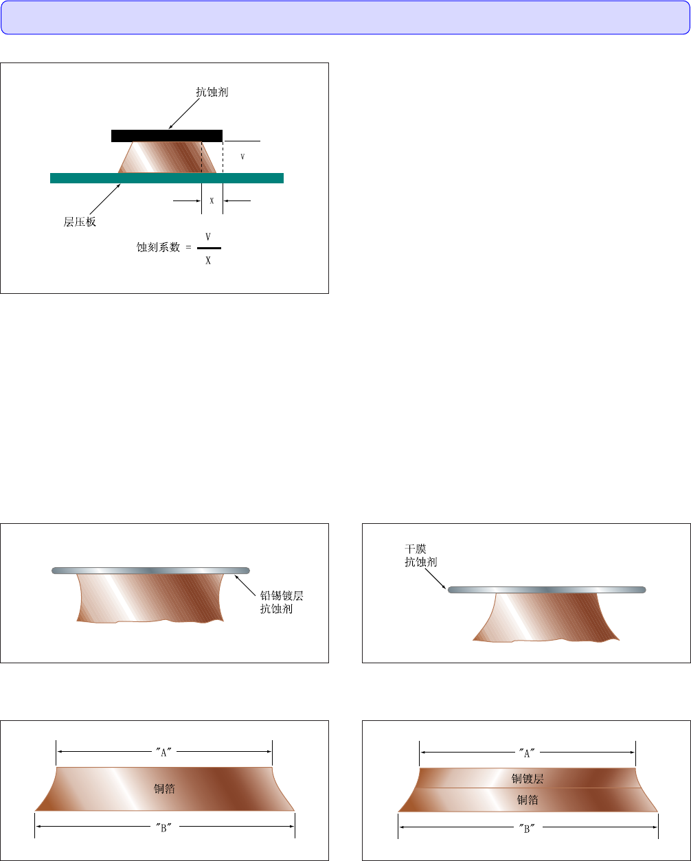
‘‘A’’ Point of Narrowest Conductor Width: This is not ‘‘Minimum
Conductor Width’’ noted on procurement documentation or perfor-
mance specifications.
‘‘B’’ Conductor Base Width: The width that is measured when
‘‘Minimum Conductor Width’’ is noted on the procurement docu-
mentation or performance specification.
‘‘C’’ Production Master Width: This width usually determines the
width of the metal or organic resist on the etched conductor.
Design width of the conductor is specified on the procurement
documentation and is most often measured at the conductor base
‘‘B’’ for compliance to ‘‘Minimum Conductor Width’’ require-
ments.
“A”导体最窄处宽度:这不是采购文件或性能规范所指的
“最小导体宽度”。
“B”导体底宽:当采购文件或性能规范标注有“最小导体
宽度”时,测量此宽度。
“C”生产底版导体宽度:这个宽度通常确定被蚀刻导体上
金属或有机抗蚀剂的宽度。
在采购文件规定导体设计宽度,通常测量导体基体底部
“B”的宽度,以确定是否符合“最小导体宽度”的要求。
The following two configurations show that conductor width may be greater at the surface than at the base:
下面两种不同导体外形图,显示导体表面的宽度可以大于底部的宽度。
图321a
图321b
热熔前的图形电镀(干膜抗蚀剂)
图321d
去膜前的全板电镀(干膜抗蚀剂)
图321c
蚀刻后的内层
图321e
用于埋孔的内层电镀层
3.2 CONDUCTIVE PATTERNS – GENERAL(导电图形 – 总则)
3.2.1 Etching Characteristics(蚀刻特性)
94 IPC-A-600H-20102010年4月
Visual observations made on cross-sections only.(仅对显微切片进行目检观察。)
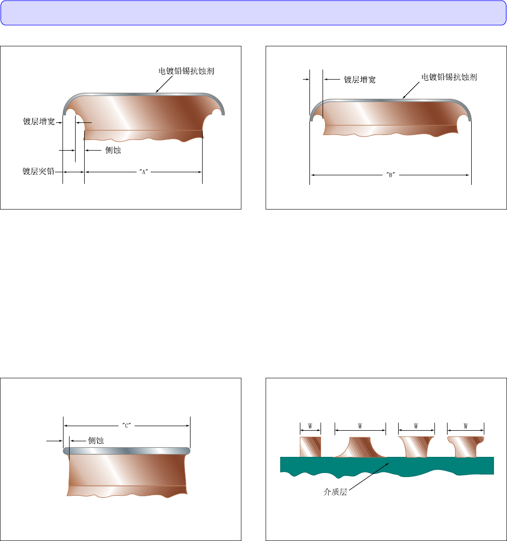
Note: The extent of outgrowth, if present, is related to the dry film resist thickness. Outgrowth occurs when the plating thickness exceeds
the resist thickness.
Note: The different etch configurations may not meet intended design requirements.
注: 镀层增宽的程度与干膜抗蚀剂的厚度有关。当镀层厚度超过抗蚀剂厚度时,就会产生镀层增宽。
注: 由于蚀刻外形的不同可能不能满足设计目的要求。
图321f
具有镀层增宽的图形电镀(干膜抗蚀剂)
图321h
具有镀层增宽的图形电镀(液态抗蚀剂)
图321g
薄铜箔与图形电镀(抗蚀剂)
图321i
随着表面阻剂W的不同,导体有效宽度与导体的宽度可能会不相同
3.2 CONDUCTIVE PATTERNS – GENERAL(导电图形 – 总则)
3.2.1 Etching Characteristics (cont.)(蚀刻特性(续))
95IPC-A-600H-2010 2010年4月
Visual observations made on cross-sections only.(仅对显微切片进行目检观察。)