IPC-A-600H-2010 中文版 印制板的可接受性 (1).pdf - 第120页
Acceptable - Class 1,2 (可接受条件 - 1,2级) • Wrap plating is continuous from the filled plated hole onto the external surface. • Wrap thickness is not less than 5 µm [197 µin] for all through- hole and via structures. • Reduc…
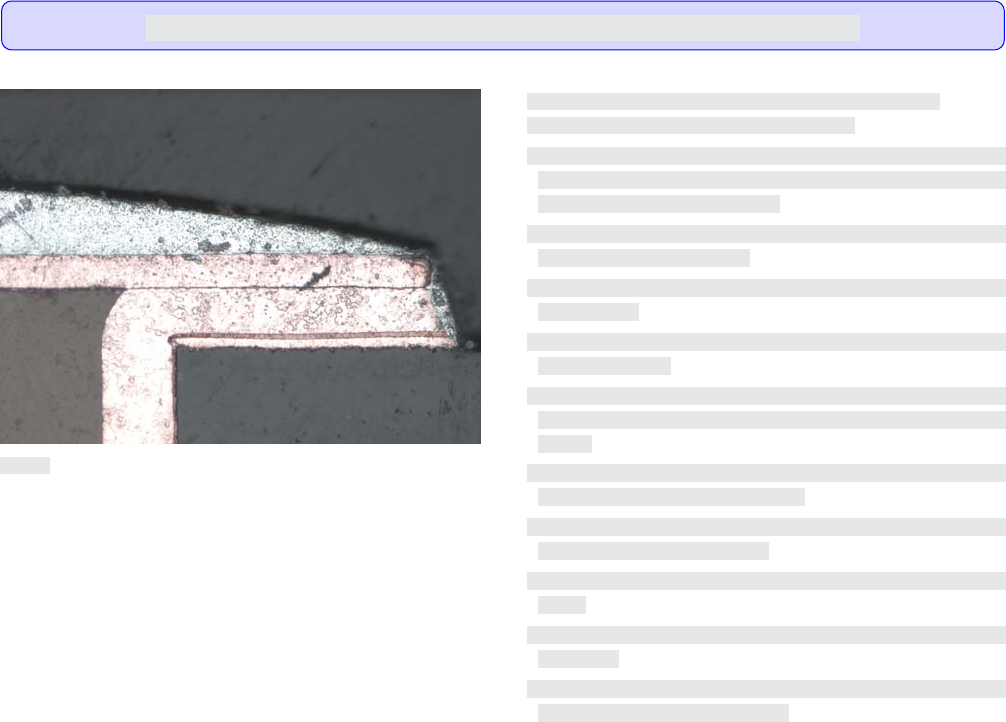
Target Condition - Class 1,2,3(⽬标条件 - 1,2,3级)
Acceptable - Class 3(可接受条件 - 3级)
• Wrap plating is continuous from the filled plated hole onto the
external surface and extends by a minimum of 25 µm [984 µin]
where an annular ring is required.
• Wrap thickness is not less than 12 µm [472 µin] for through, blind
and buried vias ≥ two layers..
• Wrap thickness is not less than 6 µm [236 µin] for blind and bur-
ied microvias.
• Wrap thickness is not less than 7 µm [276 µin] for buried via
cores (two layers).
• Reduction of surface wrap copper plating by processing (sanding,
etching, planarization, etc.) does not result in insufficient wrap
plating.
• 包覆铜电镀从填塞的镀覆孔到外层表面是连续的,且要求有
环宽时,至少延伸25µm[984µin]。
• 对于大于等于两层的通孔、盲导通孔和埋导通孔,包覆铜镀
层厚度不小于12µm[472µin]。
• 对于盲 孔 和 埋 孔 微 导通孔包覆铜镀层厚度不小于6µm[236
µin]。
• 对于埋 孔导通 孔 芯材(两层)包覆铜镀层厚度不小于7µm
[276µin]。
• 由于加工(研磨、蚀刻、整平等)导致的表面包覆铜镀层的
减少没有造成包覆铜镀层不足。
图339c
3.3 PLATED-THROUGH HOLES – GENERAL(镀覆孔 – 总则)
3.3.9 Copper Wrap Plating (cont.)(包覆铜电镀(续))
Visual observations made on cross-sections only.(仅对显微切片进行目检观察。)
111IPC-A-600H-2010 2010年4月
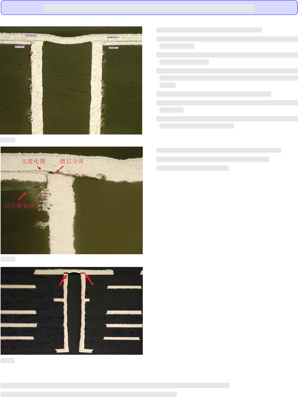
Acceptable - Class 1,2(可接受条件 - 1,2级)
• Wrap plating is continuous from the filled plated hole onto the
external surface.
• Wrap thickness is not less than 5 µm [197 µin] for all through-
hole and via structures.
• Reduction of surface wrap copper plating by processing (sanding,
etching, planarization, etc.) does not result in insufficient wrap
plating.
• 包覆电镀从填塞的镀覆孔到外层表面是连续的。
• 对于所有通孔 和 导 通 孔结构,包覆铜镀层厚度不小于5µm
[197µin]。
• 由于加工(研磨、蚀刻、整平等)导致的表面包覆铜镀层的
减少没有造成包覆铜镀层不足。
Nonconforming - Class 1,2,3(不符合条件 - 1,2,3级)
• Defects either do not meet or exceed above criteria.
• 缺陷不符合或超出上述要求。
Note: Cap plating, if required, over filled holes is not considered in wrap copper thickness measurements.
注: 如要求盖覆电镀,测量包覆铜厚度时,不考虑将塞孔上方作为测量点。
图339d
图339e
图339f
3.3 PLATED-THROUGH HOLES – GENERAL(镀覆孔 – 总则)
3.3.9 Copper Wrap Plating (cont.)(包覆铜电镀(续))
Visual observations made on cross-sections only.(仅对显微切片进行目检观察。)
112 IPC-A-600H-20102010年4月
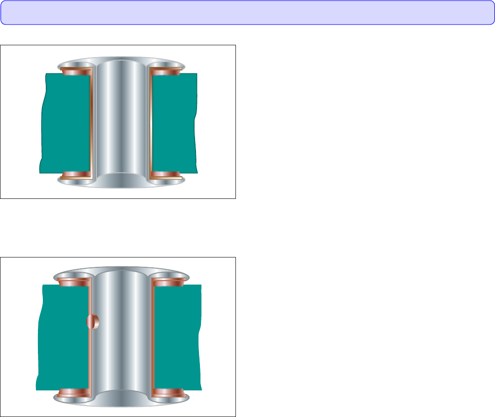
Target Condition - Class 1,2,3(⽬标条件 - 1,2,3级)
• Hole is free of voids.
• 孔内无空洞。
Acceptable - Class 2,3(可接受条件 - 2,3级)
• No more than one plating void per test coupon or production
printed board, regardless of length or size.
• No plating void in excess of 5% of the total printed board thick-
ness.
• No plating voids evident at the interface of an internal conductive
layer and plated hole wall.
• Plating voids less than or equal to 90° of the circumference.
• 每块附连测试板或成品印制板上的镀层空洞不多于1个,无
论长度或大小。
• 镀层空洞不超过印制板总厚度的5%。
• 在内层导电层与孔壁镀层的界面无镀层空洞。
• 镀层空洞小于或等于圆周的90°。
Acceptable - Class 1(可接受条件 - 1级)
• No more than three plating void per test coupon or production
printed board, regardless of length or size.
• No plating void in excess of 5% of the total printed board thick-
ness.
• No plating voids evident at the interface of an internal conductive
layer and plated hole wall.
• Plating voids less than or equal to 90° of the circumference.
• 每块附连测试板或成品印制板上的镀层空洞不多于3个,无
论长度或大小。
• 镀层空洞未超过印制板总厚度的5%。
• 在内层导电层与孔壁镀层的界面无镀层空洞。
• 镀层空洞小于或等于圆周的90°。
图3310a
图3310b
3.3 PLATED-THROUGH HOLES – GENERAL(镀覆孔 – 总则)
3.3.10 Plating Voids(镀层空洞)
113IPC-A-600H-2010 2010年4月
Visual observations made on cross-sections only.(仅对显微切片进行目检观察。)