IPC-A-600H-2010 中文版 印制板的可接受性 (1).pdf - 第76页
T arget Condition - Class 1,2,3 (⽬标条件 - 1,2,3级) • Conductor spacing meets dimensional requirements of the pro- curement documentation. • 导 体 间距 满 足采 购 文件的 尺寸 要求。 Acceptable - Class 3 (可接受条件 - 3级) • Any combination of edg…
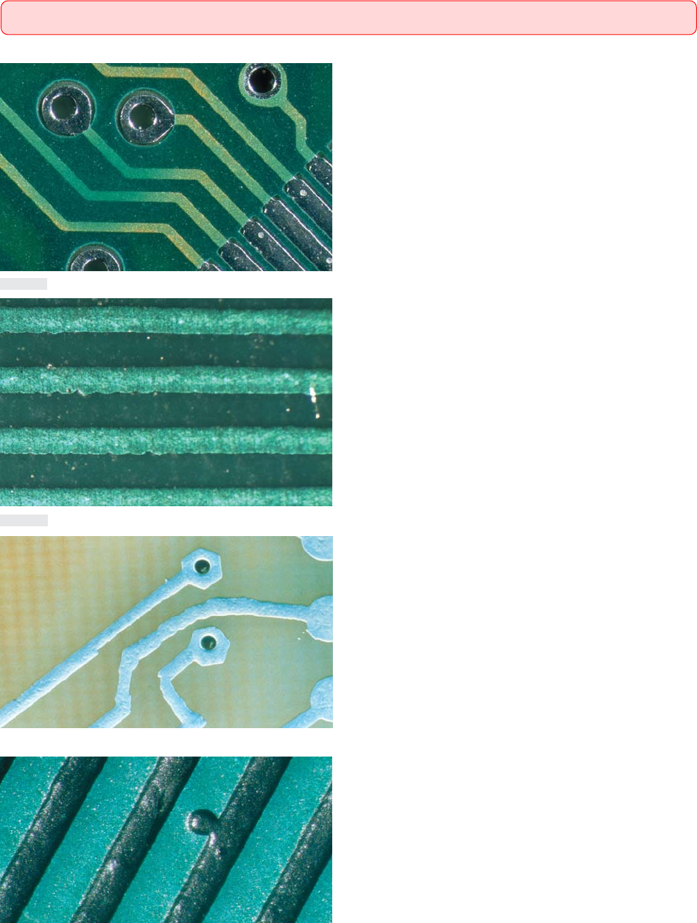
Target Condition - Class 1,2,3(⽬标条件 - 1,2,3级)
• Conductor width meets dimensional requirements of artwork or
procurement documentation.
• 导体宽度及间距满足照相底版或采购文件的尺寸要求。
Acceptable - Class 2,3(可接受条件 - 2,3级)
• Any combination of isolated edge roughness, nicks, pinholes, and
scratches exposing base material that reduces the conductor width
by 20% of the minimum value or less.
• There is no occurrence (edge roughness, nicks, etc.) greater than
10% of the conductor length or more than 13.0 mm [0.512 in],
whichever is less.
• 孤立的导体边缘粗糙、缺口、针孔及暴露基材的划伤等缺陷
的任何组合使导体宽度的减小量小于等于最小宽度的20%。
• 缺陷(边缘粗糙、缺口等)总长度不大于导体长度的10%,
或不超过13mm[0.512in],取两者中的较小者。
Acceptable - Class 1(可接受条件 - 1级)
• Any combination of isolated edge roughness, nicks, pinholes, and
scratches exposing base material that reduces the conductor width
30% of the minimum value or less.
• There is no occurrence (edge roughness, nicks, etc.) greater than
10% of the conductor length or more than 25.0 mm [0.984 in],
whichever is less.
• 孤立的导体边缘粗糙、缺口、针孔及暴露基材的划伤等缺陷
的任何组合使导体宽度的减小量小于等于最小宽度的30%。
• 缺陷(边缘粗糙、缺口等)总长度不大于导体长度的10%,
或不超过25mm[0.984in],取两者中的取较小者。
Nonconforming - Class 1,2,3(不符合条件 - 1,2,3级)
• Defects either do not meet or exceed above criteria.
• 缺陷不符合或超出上述要求。
图21011a
图21011b
图21011c
图21011d
2.10 PATTERN DEFINITION – DIMENSIONAL(图形精确度 – 尺⼨要求)
2.10.1.1 Conductor Width(导体宽度)
67IPC-A-600H-2010 2010年4月
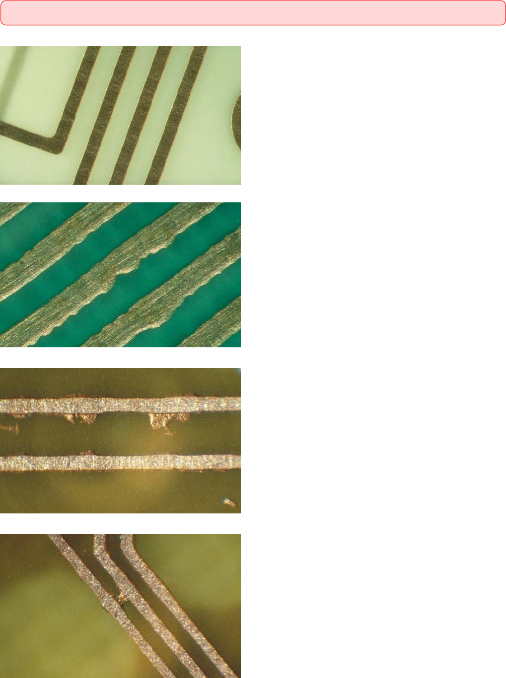
Target Condition - Class 1,2,3(⽬标条件 - 1,2,3级)
• Conductor spacing meets dimensional requirements of the pro-
curement documentation.
• 导体间距满足采购文件的尺寸要求。
Acceptable - Class 3(可接受条件 - 3级)
• Any combination of edge roughness, copper spikes, etc., that does
not reduce the specified minimum conductor spacing by more
than 20% in isolated areas.
• 任何孤立区域内导体边缘粗糙、铜刺等缺陷的任意组合未使
规定的最小导体间距的减少大于20%。
Acceptable - Class 1,2(可接受条件 - 1,2级)
• Any combination of edge roughness, copper spikes, etc., that does
not reduce the specified minimum conductor spacing by more
than 30% in isolated areas.
• 任何孤立区域内导体边缘粗糙、铜刺等缺陷的任意组合未使
规定的最小导体间距的减少大于30%。
Nonconforming - Class 1,2,3(不符合条件 - 1,2,3级)
• Defects either do not meet or exceed above criteria.
• 缺陷不符合或超出上述要求。
图21012a
图21012b
图21012c
图21012d
2.10 PATTERN DEFINITION – DIMENSIONAL(图形精确度 – 尺⼨要求)
2.10.1.2 Conductor Spacing(导体间距)
68 IPC-A-600H-20102010年4月
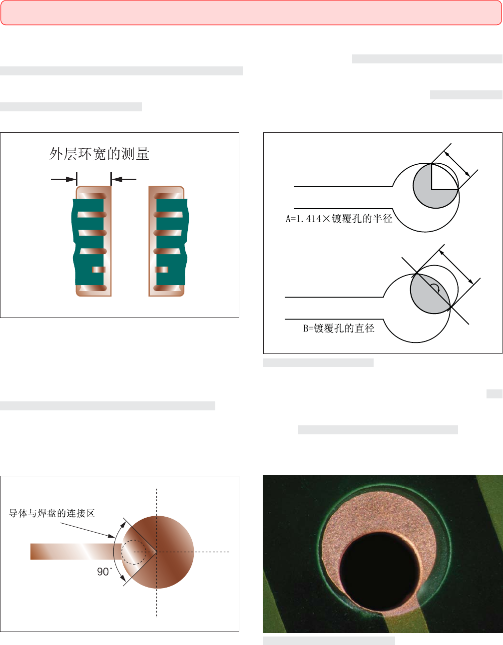
External Annular Ring: The minimum annular ring on external layers is the minimum amount of copper (at the narrowest point) between
the edge of the hole and the edge of the land after plating of the finished hole (see Figure 2102a). Hole breakout refers to a condition where
a hole is not completely surrounded by the land (see Figure 2102b).
外层环宽:外层的最小环宽是成品孔在电镀后孔边缘和焊盘边缘之间(最窄处)的最小量的铜(见图2102a)。孔的破环指孔未被
焊盘完全包围的状况(见图2101b)。
Conductor to Land Junction: A 90° area centered around the point where the conductor connects to the land (see Figure 2102c). This
area only applies to breakout conditions (see Figure 2102d).
导体与焊盘的连接区:以导体与焊盘连接点为中心的90°区域(见图2102c)。该区域仅适用于破环的状况(见2102d)。
图2102a 外层环宽
图2102b 90°和180°的破环
B
A
180°
90°
图2102c 导体与焊盘的连接区 图2102d 导体与焊盘连接处的破环
2.10 PATTERN DEFINITION – DIMENSIONAL(图形精确度 – 尺⼨要求)
2.10.2 External Annular Ring – Measurement(外层环宽的测量)
69IPC-A-600H-2010 2010年4月