IPC-A-600H-2010 中文版 印制板的可接受性 (1).pdf - 第62页
T arget Condition - Class 1,2,3 (⽬标条件 - 1,2,3级) • No solder mask misregistration. The solder mask is centered around the lands within the nominal regis- tration spacings. • 未 出现 阻 焊 膜 错 位 。 阻 焊 膜 在标 称 的 重 合 度间 距 内,以 焊 盘 …
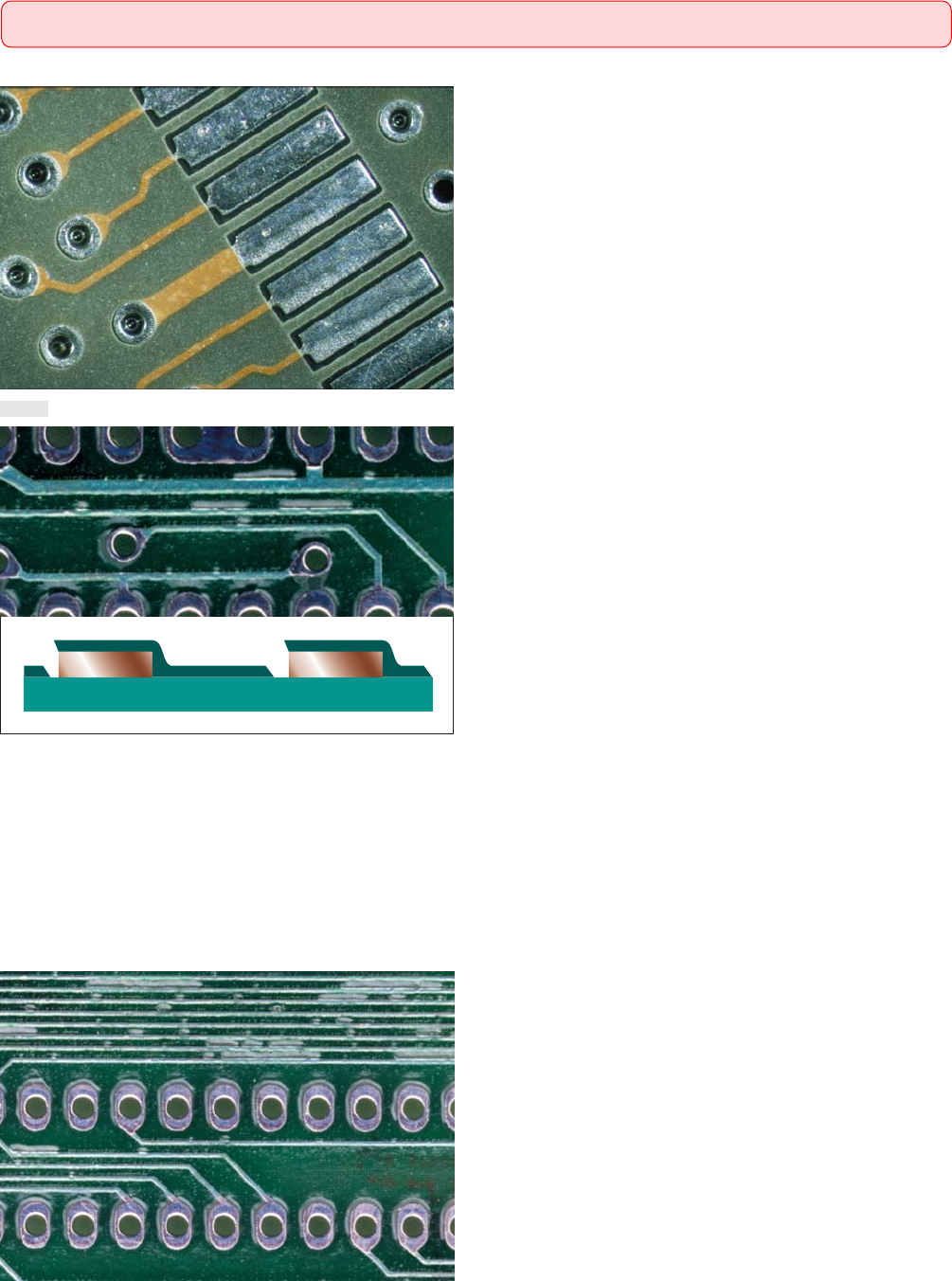
Target Condition - Class 1,2,3(⽬标条件 - 1,2,3级)
• The solder mask exhibits uniform appearance over the base mate-
rial surface, conductor sides and edges. It is firmly bonded to the
printed board surface with no visible skipping, voids or other
defects.
• 阻焊膜在基材表面、导体侧面和边缘处都呈现均匀的外表,
并已牢固粘接在印制板表面上,无可见的跳印、空洞或其它
缺陷。
Acceptable - Class 2,3(可接受条件 - 2,3级)
• In areas containing parallel conductors, adjacent conductors are
not exposed by the absence of solder mask except where space
between conductors is intended to be exposed.
• Touch up, if required to cover these areas with solder mask, is of
a material that is compatible to and of equal resistance to solder-
ing and cleaning as the originally applied solder mask.
• 在有平行导体的区域内,除了导体之间有意不覆盖阻焊剂处
外,没有由于缺少阻焊剂而使相邻导体暴露。
• 如要求用阻焊膜修补以覆盖这些区域时,使用与最初使用的
阻焊剂相兼容的并具有同等耐焊接性和耐清洗性的材料。
Acceptable - Class 1(可接受条件 - 1级)
• The missing solder mask does not reduce the conductor spacing
between conductive patterns below the minimum acceptability
requirements.
• There is skipping of the solder mask along the sides of the con-
ductive patterns.
• 缺失的阻焊膜未使导体间的间距减少至低于最小可接收性要
求。
• 沿着导电图形侧边可有跳印的阻焊膜。
Nonconforming - Class 1,2,3(不符合条件 - 1,2,3级)
• Defects either do not meet or exceed above criteria.
• 缺陷不符合或超出上述要求。
图291a
图291b
图291c
2.9 SOLDER MASK(阻焊膜(阻焊剂))
2.9.1 Coverage Over Conductors (Skip Coverage)(导体上的覆盖(跳印))
53IPC-A-600H-2010 2010年4月
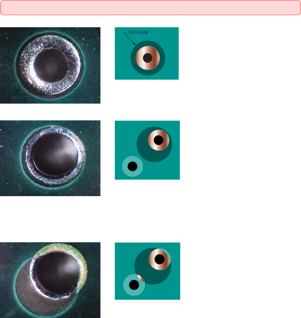
Target Condition - Class 1,2,3
(⽬标条件 - 1,2,3级)
• No solder mask misregistration. The solder mask is
centered around the lands within the nominal regis-
tration spacings.
• 未出现阻焊膜错位。阻焊膜在标称的重合度间
距内,以焊盘为中心环绕在其周围。
Acceptable - Class 1,2,3
(可接受条件 - 1,2,3级)
• Misregistration of the mask to the land patterns but
the solder mask does not violate minimum annular
ring requirements.
• No solder mask in PTHs, except those not intended
for soldering.
• Adjacent, electrically isolated lands or conductors
are not exposed.
• 阻焊膜图形与焊盘错位,但不违反最小环宽要
求。
• 除那些无需焊接的孔外,镀覆孔内无阻焊膜。
• 未暴露相互电气隔离的相邻焊盘或导体。
Nonconforming - Class 1,2,3
(不符合条件 - 1,2,3级)
• Defects either do not meet or exceed above criteria.
• 缺陷不符合或超出上述要求。
图292a
图292c
图292e
图292b
图292d
图292f
2.9 SOLDER MASK(阻焊膜(阻焊剂))
2.9.2 Registration to Holes (All Finishes)(与孔的重合度(所有涂覆层))
54 IPC-A-600H-20102010年4月
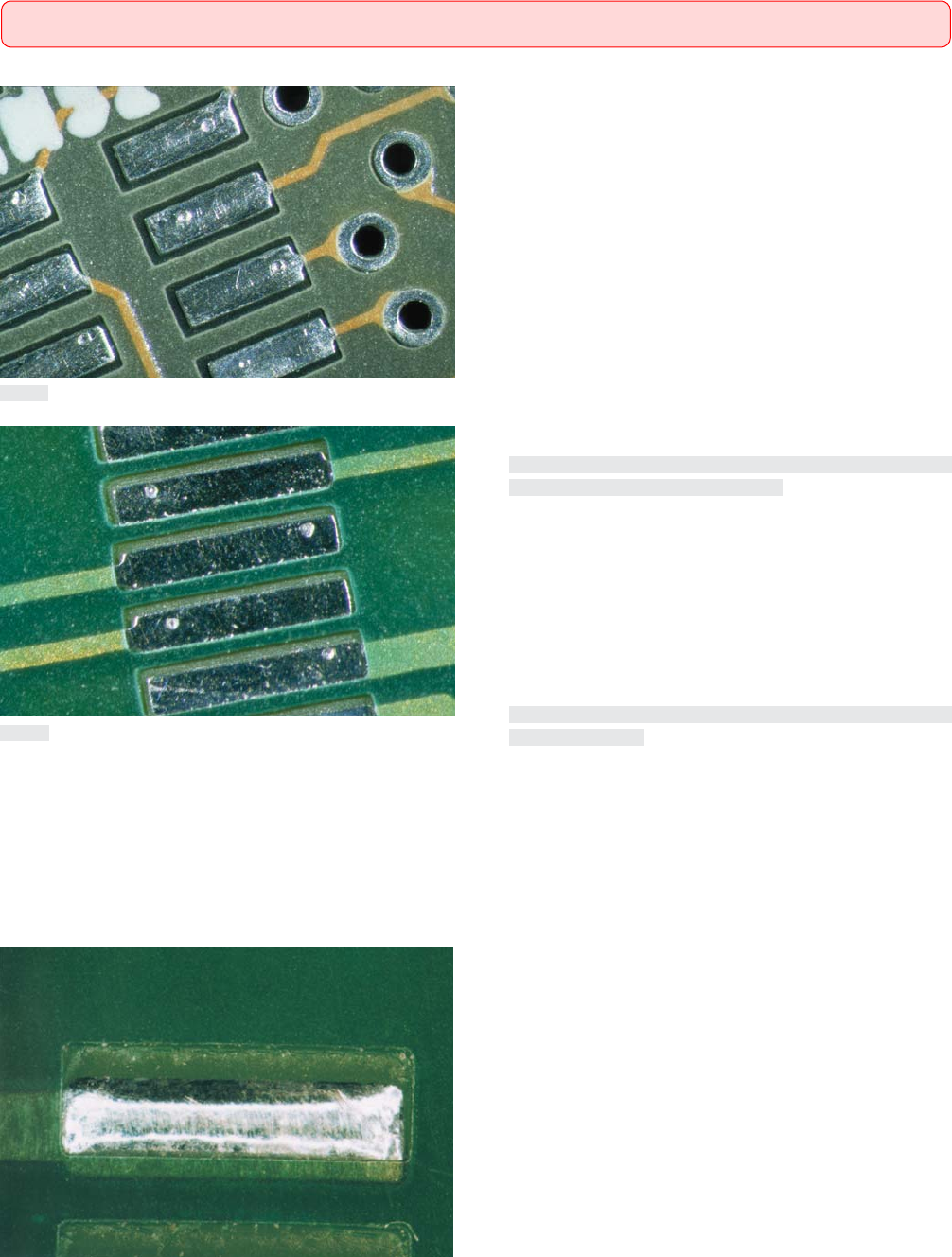
Target Condition - Class 1,2,3(⽬标条件 - 1,2,3级)
• No solder mask misregistration.
• 未出现阻焊膜错位。
Acceptable - Class 1,2,3(可接受条件 - 1,2,3级)
• Misregistration to copper-defined lands does not expose adjacent,
electrically isolated lands or conductors.
• No solder mask encroachment on edge board printed contacts or
test points.
• On surface mount lands with a pitch of 1.25 mm [0.04921 in] or
greater, encroachment is on one side of land only and does not
exceed 0.05 mm [0.0020 in].
• On surface mount lands with a pitch less than 1.25 mm [0.04921
in], encroachment is on one side of land only and does not exceed
0.025 mm [0.000984 in].
• 阻焊膜与铜箔限定的焊盘之间的错位没有暴露相邻的电气隔
离的焊盘或导体。
• 阻焊膜没有侵占板边印制接触片或测试点。
• 对于节距大于或等于1.25mm[0.04921in]的表面贴装焊盘,只
能侵占焊盘的一侧,且不超过0.05mm[0.0020in]。
• 对于节距小于1.25mm[0.04921in]的表面贴装焊盘,只能侵占
焊盘的一侧,且不超过0.025mm[0.000984in]。
Nonconforming - Class 1,2,3(不符合条件 - 1,2,3级)
• Defects either do not meet or exceed above criteria.
• 缺陷不符合或超出上述要求。
图293a
图293b
图293c
2.9 SOLDER MASK(阻焊膜(阻焊剂))
2.9.3 Registration to Other Conductive Patterns(与其它导电图形的重合度)
55IPC-A-600H-2010 2010年4月