IPC-A-600H-2010 中文版 印制板的可接受性 (1).pdf - 第64页
Solder Mask-Defined Lands: A portion of the conductive pattern, used to connect electronic component ball terminations, (BGAs, Fine- Pitch BGAs, etc.), where the solder mask encroaches on the edges of the land to restric…
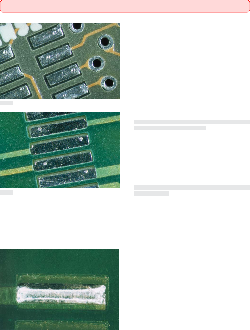
Target Condition - Class 1,2,3(⽬标条件 - 1,2,3级)
• No solder mask misregistration.
• 未出现阻焊膜错位。
Acceptable - Class 1,2,3(可接受条件 - 1,2,3级)
• Misregistration to copper-defined lands does not expose adjacent,
electrically isolated lands or conductors.
• No solder mask encroachment on edge board printed contacts or
test points.
• On surface mount lands with a pitch of 1.25 mm [0.04921 in] or
greater, encroachment is on one side of land only and does not
exceed 0.05 mm [0.0020 in].
• On surface mount lands with a pitch less than 1.25 mm [0.04921
in], encroachment is on one side of land only and does not exceed
0.025 mm [0.000984 in].
• 阻焊膜与铜箔限定的焊盘之间的错位没有暴露相邻的电气隔
离的焊盘或导体。
• 阻焊膜没有侵占板边印制接触片或测试点。
• 对于节距大于或等于1.25mm[0.04921in]的表面贴装焊盘,只
能侵占焊盘的一侧,且不超过0.05mm[0.0020in]。
• 对于节距小于1.25mm[0.04921in]的表面贴装焊盘,只能侵占
焊盘的一侧,且不超过0.025mm[0.000984in]。
Nonconforming - Class 1,2,3(不符合条件 - 1,2,3级)
• Defects either do not meet or exceed above criteria.
• 缺陷不符合或超出上述要求。
图293a
图293b
图293c
2.9 SOLDER MASK(阻焊膜(阻焊剂))
2.9.3 Registration to Other Conductive Patterns(与其它导电图形的重合度)
55IPC-A-600H-2010 2010年4月

Solder Mask-Defined Lands: A portion of the conductive pattern, used to connect electronic component ball terminations, (BGAs, Fine-
Pitch BGAs, etc.), where the solder mask encroaches on the edges of the land to restrict the ball attachment within the solder mask profile.
阻焊膜限定的焊盘:导电图形的一部分,用来连接电子元器件的球形端子(BGA、细节距BGA等),阻焊膜侵占到焊盘的边缘,
从而将球形连接限制在阻焊膜围绕的范围内。
Target Condition - Class 1,2,3(⽬标条件 - 1,2,3级)
• The solder mask overlap is centered around the lands.
• 阻焊膜与焊盘的重叠区以焊盘为中心,环绕在其周围。
Acceptable - Class 1,2,3(可接受条件 - 1,2,3级)
• Misregistration creates breakout of the solder mask on the land of
not more than 90°.
• 错位使阻焊膜在焊盘上的破出区域不超过90°。
Nonconforming - Class 1,2,3(不符合条件 - 1,2,3级)
• Defects either do not meet or exceed above criteria.
• 缺陷不符合或超出上述要求。
图2931a
2.9 SOLDER MASK(阻焊膜(阻焊剂))
2.9.3.1 Ball Grid Array (Solder Mask-Defined Lands)(球栅列阵(阻焊膜限定的焊盘))
56 IPC-A-600H-20102010年4月
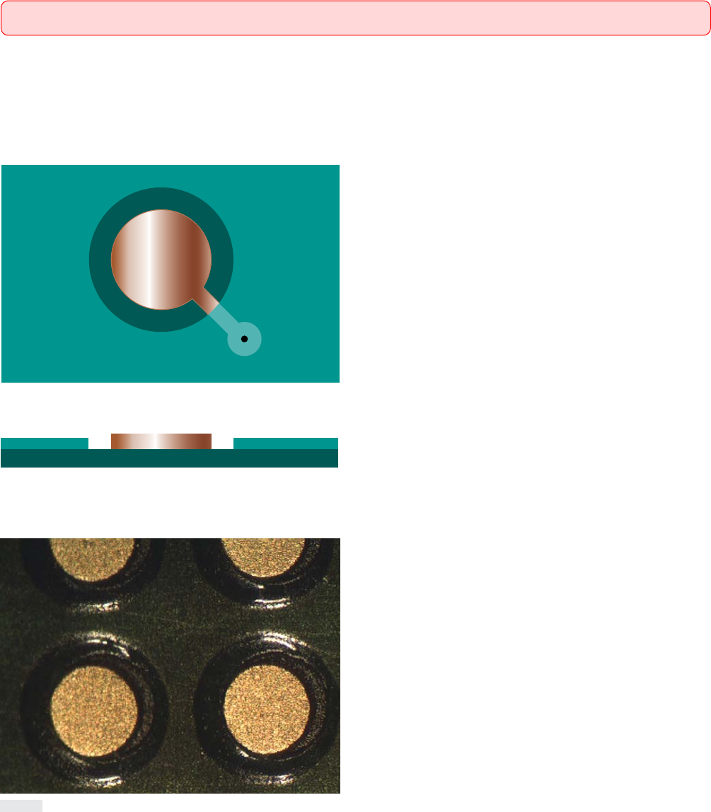
Copper-Defined Lands: A portion of the conductive pattern usually, but not exclusively, used for the connection and/or attachment of
components where the land metal is involved in the attachment process, and if solder mask is applied to the product a clearance is provided
for the land area.
铜箔限定的焊盘:通常(但并非一定)为导电图形的一部分,在焊接过程中,焊盘金属用来连接和/或焊接元器件,如果产品涂
覆阻焊膜,则焊盘区周围留有间隙。
Target Condition - Class 1,2,3(⽬标条件 - 1,2,3级)
• The solder mask is centered around the copper land with clear-
ance.
• 阻焊膜以铜焊盘为中心,环绕其周围并留有间隙。
Acceptable - Class 1,2,3(可接受条件 - 1,2,3级)
• Solder mask does not encroach on the land, except at the conduc-
tor attachment.
• 除了导体连接处外,阻焊膜未涂覆侵占到焊盘上。
Nonconforming - Class 1,2,3(不符合条件 - 1,2,3级)
• Defects either do not meet or exceed above criteria.
• 缺陷不符合或超出上述要求。
图2932a
图2932b
2.9 SOLDER MASK(阻焊膜(阻焊剂))
2.9.3.2 Ball Grid Array (Copper-Defined Lands)(球栅列阵(铜箔限定的焊盘))
57IPC-A-600H-2010 2010年4月