IPC-A-600H-2010 中文版 印制板的可接受性 (1).pdf - 第66页
Solder Dam: A portion of the solder mask pattern, used in conjunction with BGA or Fine Pitch BGA mounting, that provides a segment of solder mask material to separate the mounting portion of the pattern and the interconn…
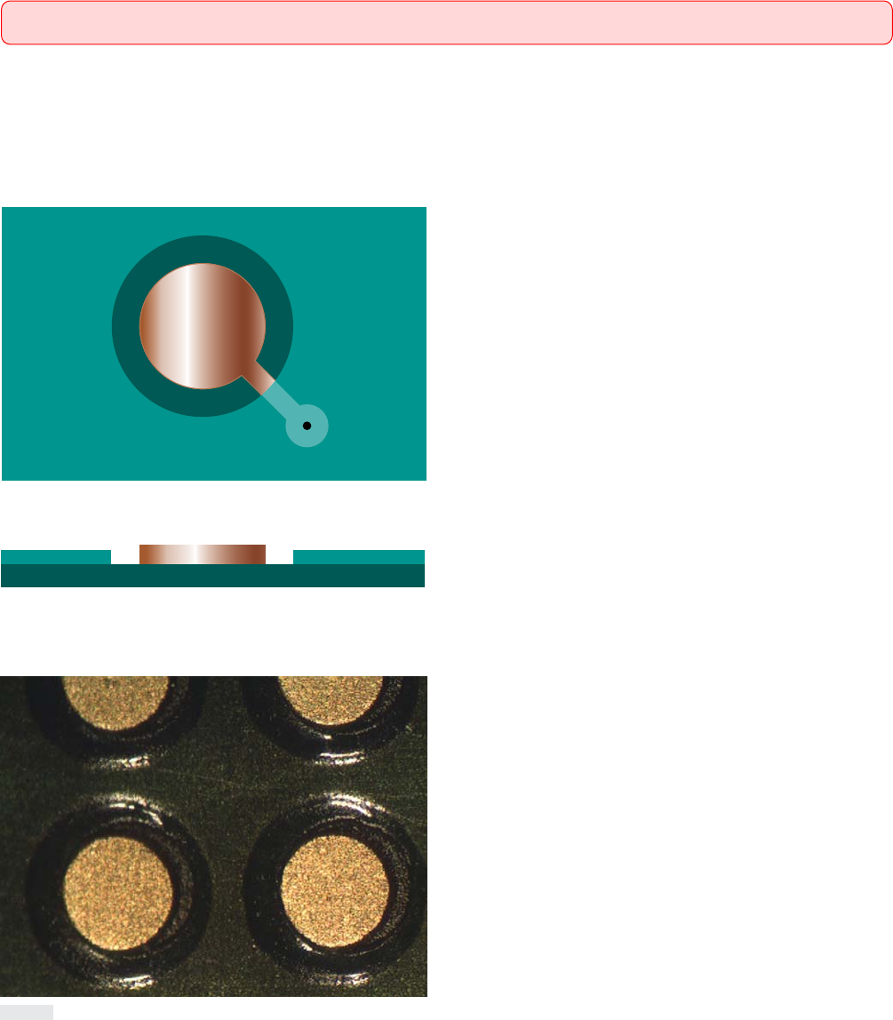
Copper-Defined Lands: A portion of the conductive pattern usually, but not exclusively, used for the connection and/or attachment of
components where the land metal is involved in the attachment process, and if solder mask is applied to the product a clearance is provided
for the land area.
铜箔限定的焊盘:通常(但并非一定)为导电图形的一部分,在焊接过程中,焊盘金属用来连接和/或焊接元器件,如果产品涂
覆阻焊膜,则焊盘区周围留有间隙。
Target Condition - Class 1,2,3(⽬标条件 - 1,2,3级)
• The solder mask is centered around the copper land with clear-
ance.
• 阻焊膜以铜焊盘为中心,环绕其周围并留有间隙。
Acceptable - Class 1,2,3(可接受条件 - 1,2,3级)
• Solder mask does not encroach on the land, except at the conduc-
tor attachment.
• 除了导体连接处外,阻焊膜未涂覆侵占到焊盘上。
Nonconforming - Class 1,2,3(不符合条件 - 1,2,3级)
• Defects either do not meet or exceed above criteria.
• 缺陷不符合或超出上述要求。
图2932a
图2932b
2.9 SOLDER MASK(阻焊膜(阻焊剂))
2.9.3.2 Ball Grid Array (Copper-Defined Lands)(球栅列阵(铜箔限定的焊盘))
57IPC-A-600H-2010 2010年4月
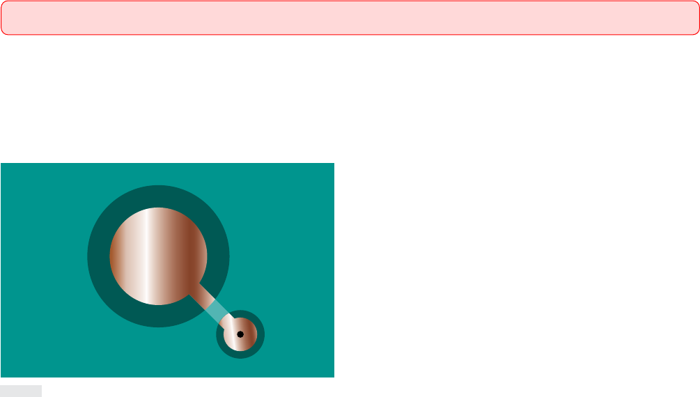
Solder Dam: A portion of the solder mask pattern, used in conjunction with BGA or Fine Pitch BGA mounting, that provides a segment
of solder mask material to separate the mounting portion of the pattern and the interconnection via in order to avoid solder being skived from
the attachment joint into the via.
阻焊坝:阻焊图形的一部分,用于BGA或细节距BGA贴装连接,以一小段阻焊材料将图形的贴装部分与互连导通孔隔开,以避免
焊料从焊接处落入导通孔内。
Target Condition - Class 1,2,3(⽬标条件 - 1,2,3级)
• The solder mask is centered around the copper land and escape
via with clearance. Mask only covers the conductor between cop-
per land and escape via.
• 阻焊膜分别以铜焊盘和导通孔为中心,并留有余隙。阻焊膜
仅覆盖铜焊盘与导通孔间的导体。
Acceptable - Class 1,2,3(可接受条件 - 1,2,3级)
• If solder mask dam is specified (to prevent bridging of solder to
the via), it remains in place with the copper covered.
• 若规定有阻焊坝(为防止焊料与导通孔的桥连),阻焊坝保
留在规定位置,且铜被覆盖。
Nonconforming - Class 1,2,3(不符合条件 - 1,2,3级)
• Defects either do not meet or exceed above criteria.
• 缺陷不符合或超出上述要求。
图2933a
2.9 SOLDER MASK(阻焊膜(阻焊剂))
2.9.3.3 Ball Grid Array (Solder Dam)(球栅列阵(阻焊坝))
58 IPC-A-600H-20102010年4月
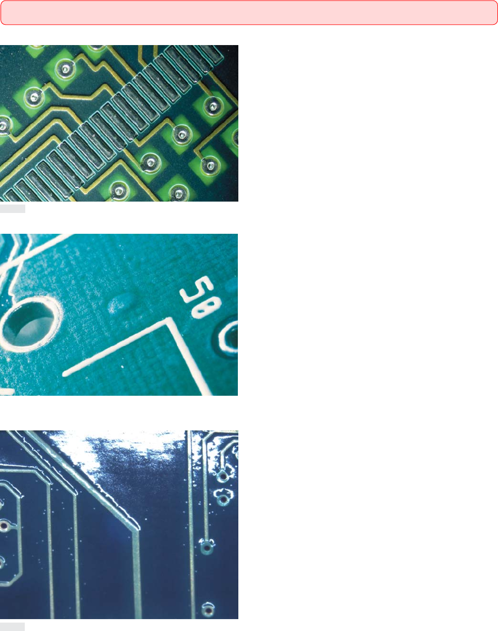
Target Condition - Class 1,2,3(⽬标条件 - 1,2,3级)
• No evidence of blisters, bubbles or delamination between the sol-
der mask and the printed board base material and conductive pat-
terns.
• 阻 焊 膜 和印制板基材及导电图形之间无起泡、气泡或分层
迹象。
Acceptable - Class 2,3(可接受条件 - 2,3级)
• Two per side not exceeding 0.25 mm [0.00984 in] in the greatest
dimension.
• Reduction of electrical spacing does not exceed 25%, or the mini-
mum spacing.
• 印制板每面可有两个瑕疵,每个瑕疵的最大尺寸不超过0.25
mm[0.009841in]。
• 电气间距的减少量不超过间距的25%,或减少后的电气间距
不小于最小间距。
Acceptable - Class 1(可接受条件 - 1级)
• Blisters, bubbles or delamination do not bridge between conduc-
tors.
• 起泡、气泡或分层没有使导体桥连。
图294a
图294b
图294c
2.9 SOLDER MASK(阻焊膜(阻焊剂))
2.9.4 Blisters/Delamination(起泡/分层)
59IPC-A-600H-2010 2010年4月