IPC-A-600H-2010 中文版 印制板的可接受性 (1).pdf - 第99页
This section covers acceptability requirements for printed board etching, innerlayers, and impedance controlled products. An acceptable etching process must result in all residual metal being removed with no evidence of …
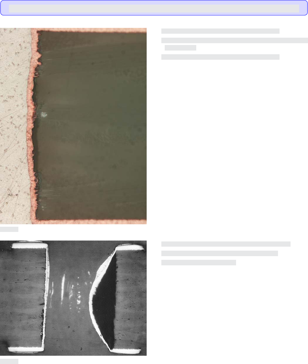
Acceptable - Class 1,2,3(可接受条件 - 1,2,3级)
• Dimensional and plating requirements of IPC-6010 performance
series are met.
• 尺寸和镀层满足IPC-6010性能系列文件的要求。
Nonconforming - Class 1,2,3(不符合条件 - 1,2,3级)
• Defects either do not meet or exceed above criteria.
• 缺陷不符合或超出上述要求。
图3110a
图3110b
3.1 DIELECTRIC MATERIALS(介质材料)
3.1.10 Hole Wall Dielectric/Plated Barrel Separation (Hole Wall Pullaway)(孔壁介质与孔壁镀层分离(孔壁拉脱))
Visual observations made on cross-sections only.(仅对显微切片进行目检观察。)
90 IPC-A-600H-20102010年4月

This section covers acceptability requirements for printed board etching, innerlayers, and impedance controlled products. An acceptable
etching process must result in all residual metal being removed with no evidence of contamination remaining on the product.
Over etching is cause for rejection when potential slivers result from excessive overhang of metal resist plating or when the finished conduc-
tor widths are less than specification requirements.
Under etching is cause for rejection when spurious metal remains on the product to the extent that spacing between conductors is less than
specification requirements or if conductor width requirements are exceeded.
Conductor width is defined as the observable width of the copper conductor excluding organic or metallic resists unless otherwise specified.
The ‘‘Minimum Conductor Width’’ often specified on the procurement documentation or performance document is usually measured at the
base of the conductor and may not be the actual narrowest width of the conductor when observed in cross section or often when viewed from
the surface. An observation from the surface may not be adequate for acceptance of some products and etching processes. Where resistance
per unit length is a requirement, a measurement of the average width of the cross-sectional area may be necessary. Where impedance control
is required, a determination of the maximum conductor width may be important for the calculating impedance and a cross-section is often
required.
Considerable variation in etch configurations is possible due to different etchants, resists and plated metal thicknesses. The conductor width
may increase or decrease from the production artwork due to techniques used in processing during the imaging and developing operations.
To achieve the ‘‘Design Width of Conductor,’’ the production master artwork often has conductor width adjustments made during plotting.
The amount of adjustment of a conductor width on the ‘‘Production Master’’ may be 0.025 to 0.05 mm [0.001 to 0.0020 in]. Determination
of adjustment is made by experimentation and compensation for an increase or decrease of the conductor width during plating or etching.
The illustrations in 3.2.1 are intended as a guideline to illustrate some of the edge geometry conditions which may result from different pro-
cessing methods and illustrate the configurations of ‘‘Outgrowth,’’ ‘‘Undercut’’ and ‘‘Overhang.’’
3.2 CONDUCTIVE PATTERNS – GENERAL(导电图形 – 总则)
Introduction(引⾔)
91IPC-A-600H-2010 2010年4月

本节涵盖了印制板的蚀刻、内层和阻抗可控产品的可接受性要求。可接受的蚀刻工艺必须保证产品上所有多余金属已被除去且没
有留下污染的痕迹。
如果过度蚀刻引起金属抗蚀镀层过大的突沿而产生潜在的金属镀屑,或者造成完工的导体宽度小于规定的要求,则过度蚀刻是拒
收的理由。
如果蚀刻不足而造成产品上产生的金属残留物使导体之间的间距小于规定的要求,或者导体宽度超过了规定的要求,蚀刻不足也
是引起拒收的理由。
除非另有规定,导体宽度是指可观察到的铜导体宽度,但不包括有机的或金属的抗蚀层。采购文件或性能文件中规定的“最小导
体宽度”通常是在导体的基底处测量的,而不是按显微切片所观察到的或通常从表面所观察到的实际最窄宽度。从表面观察不能
作为一些产品和蚀刻工艺的验收依据。当导体的单位长度电阻有要求时,则可能有必要对导体横截面的平均宽度进行测量。当有
阻抗控制要求时,最大导体宽度的测定对计算阻抗可能很重要,同时往往要求对导体进行剖切。
由于蚀刻剂、抗蚀剂和金属镀层的厚度的不同,蚀刻后图形的变异可能相当大。同时在成像和显影操作过程中由于采用的工艺技
术的不同,也会使导体宽度可能比生产底片的宽度大或小。为了达到“导体设计宽度”,在光绘生产底版的过程中往往要调整导
体的宽度。对“生产底版”导体宽度的调整量可从0.025mm至0.05mm[0.000984in至0.0020in]。尺寸的调整通过电镀或蚀刻过程的
导体宽度增大或减小程度的实验而加以确定。
3.2.1节中的示意图用来表明不同的加工方法可能产生的几种导体边缘的几何形状,并图示了“镀层增宽”、“侧蚀”和“镀层突
沿”等不同外形。
3.2
CONDUCTIVE
PATTERNS – GENERAL(导电图形 – 总则)
Introduction(引⾔)
92 IPC-A-600H-20102010年4月