IPC-A-600H-2010 中文版 印制板的可接受性 (1).pdf - 第31页
Acceptable - Class 1 (可接受条件 - 1级) • The imperfection does not reduce the conductor spacing below the minimum. • No propagation as a result of thermal testing that replicates the manufacturing process. • Crazing at the ed…
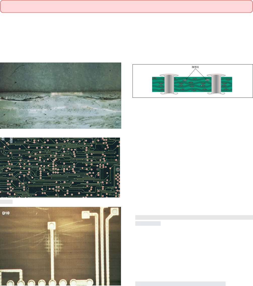
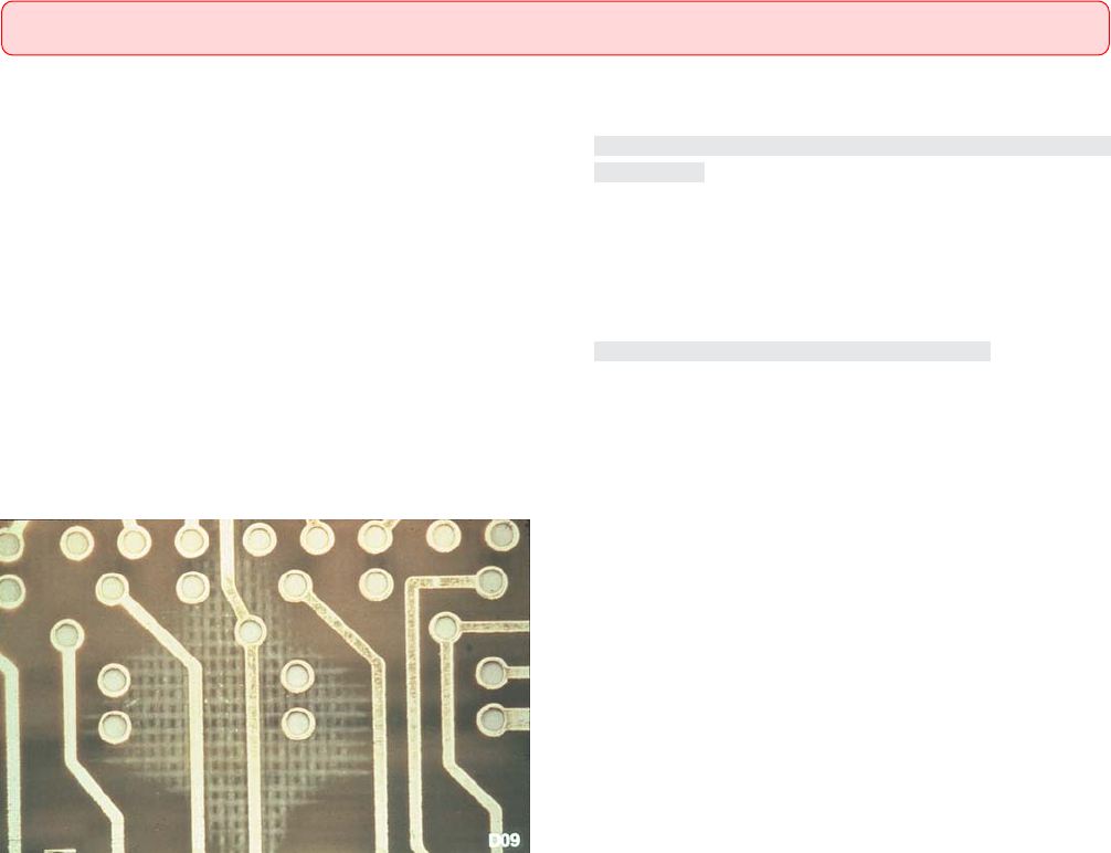
Crazing: An internal condition occurring in the laminated base material in which the fibers within the yarn are separated. This can occur at
the weave intersections or along the length of the yarn. This condition manifests itself in the form of connected white spots or ‘‘crosses’’
below the surface of the base material, and is usually related to mechanically induced stress. When the crosses are connected the condition is
evaluated as follows:
微裂纹:层压基材内纤维发生分离的一种内部状况。微裂纹可在纤维交织处或沿纤维丝长度方向出现。微裂纹状况表现为基材表
面下相连的白点或“十字纹”,通常与机械应力有关。当十字纹相互连接时,微裂纹状况评定如下:
Target Condition - Class 1,2,3(⽬标条件 - 1,2,3级)
• No evidence of crazing.
• 无微裂纹迹象。
Acceptable - Class 2,3(可接受条件 - 2,3级)
• The imperfection does not reduce the conductor spacing below
the minimum.
• The distance of crazing does not span more than 50% of the dis-
tance between adjacent conductive patterns that are not electri-
cally common.
• No propagation as a result of thermal testing that replicates the
manufacturing process.
• Crazing at the edge of the printed board does not reduce the mini-
mum distance between printed board edge and conductive pat-
tern; or more than 2.5 mm [0.0984 in] if not specified.
• 瑕疵未使导体间距减少至低于最小导体间距。
• 微裂 纹 的 跨 距 不大于相邻非电气共接导电图形之间距离的
50%。
• 没有因为模拟制造过程的热测试而扩大。
• 印制板边的微裂纹未减少板边与导电图形间的最小距离,若
未规定最小距离时,则微裂纹不大于2.5mm[0.0984in]。
Note: Crazing is observed from the surface. Cross-sections are for illustration purposes only.
注:
微裂纹可从表面观察。剖面图仅用于图示。
图232b
注:此图仅⽤作说明状况,并不要求做显微剖切评价。
图232d
图232a
图232c
2.3 BASE MATERIAL SUBSURFACE(基材表⾯下)
2.3.2 Crazing(微裂纹)
22 IPC-A-600H-20102010年4月
Acceptable - Class 1(可接受条件 - 1级)
• The imperfection does not reduce the conductor spacing below
the minimum.
• No propagation as a result of thermal testing that replicates the
manufacturing process.
• Crazing at the edge of the printed board does not reduce the mini-
mum distance between printed board edge and conductive pat-
tern; or more than 2.5 mm [0.0984 in] if not specified.
• 瑕疵未使导体间距减少至低于最小导体间距。
• 没有由于模拟制造过程的热测试而扩大。
• 印制板边的微裂纹未减少板边与导电图形间的最小距离,若
未规定最小距离时,则微裂纹不大于2.5mm[0.0984in]。
Nonconforming - Class 1,2,3(不符合条件 - 1,2,3级)
• Defects either do not meet or exceed above criteria.
• 缺陷不符合或超出上述要求。
图232e
2.3 BASE MATERIAL SUBSURFACE(基材表⾯下)
2.3.2 Crazing (cont.)(微裂纹(续))
23IPC-A-600H-2010 2010年4月
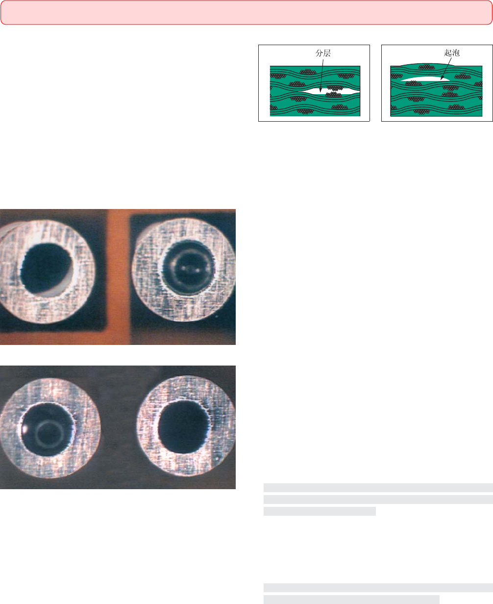
Delamination: A separation between plies within a base mate-
rial, between a material and conductive foil, or any other planar
separations within a printed board.
分层:出现在基材内的层与层之间、基材与导电箔之间,或
印制板任何其它层内的分离现象。
Blister: Delamination in the form of a localized swelling and
separation between any of the layers of a lamination base material,
or between base material and conductive foil or protective coating.
起泡:表现为层压基材的任意层之间或者基材与导电箔或保
护性涂覆层之间的局部膨胀和分离的分层。
Target Condition - Class 1,2,3(⽬标条件 - 1,2,3级)
• No blistering or delamination.
• 无起泡或分层。
Acceptable - Class 2,3(可接受条件 - 2,3级)
• The area affected by imperfections does not exceed 1% of the
printed board area on each side.
• The imperfection does not reduce the space between conductive
patterns below the minimum conductor spacing.
• The blister or delamination does not span more than 25% of the
distance between adjacent conductive patterns.
• No propagation as a result of thermal testing that replicates the
manufacturing process.
• The imperfection does not exceed the specified minimum dis-
tance between printed board edge and conductive pattern, or 2.5
mm [0.0984 in] if not specified.
• 受瑕疵影响的面积不超过印制板每面面积的1%。
• 瑕疵没有使导电图形间的间距减少至低于最小导体间距。
• 起泡或分层的跨距不大于相邻导电图形之间距离的25%。
• 没有由于模拟制造制程的热应力测试而扩大。
• 瑕疵未减少板边与导电图形间规定的最小距离,若未规定最
小距离时,则微裂纹不大于2.5mm[0.0984in]。
图233a
注:此图仅⽤作说明状况,并不要求做显微剖切评价。
图233b
图233c
2.3 BASE MATERIAL SUBSURFACE(基材表⾯下)
2.3.3 Delamination/Blister(分层/起泡)
24 IPC-A-600H-20102010年4月