IPC-A-600H-2010 中文版 印制板的可接受性 (1).pdf - 第103页
Note: The extent of outgrowth, if present, is related to the dry film resist thickness. Outgrowth occurs when the plating thickness exceeds the resist thickness. Note: The different etch configurations may not meet inten…
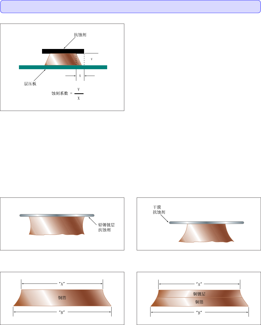
‘‘A’’ Point of Narrowest Conductor Width: This is not ‘‘Minimum
Conductor Width’’ noted on procurement documentation or perfor-
mance specifications.
‘‘B’’ Conductor Base Width: The width that is measured when
‘‘Minimum Conductor Width’’ is noted on the procurement docu-
mentation or performance specification.
‘‘C’’ Production Master Width: This width usually determines the
width of the metal or organic resist on the etched conductor.
Design width of the conductor is specified on the procurement
documentation and is most often measured at the conductor base
‘‘B’’ for compliance to ‘‘Minimum Conductor Width’’ require-
ments.
“A”导体最窄处宽度:这不是采购文件或性能规范所指的
“最小导体宽度”。
“B”导体底宽:当采购文件或性能规范标注有“最小导体
宽度”时,测量此宽度。
“C”生产底版导体宽度:这个宽度通常确定被蚀刻导体上
金属或有机抗蚀剂的宽度。
在采购文件规定导体设计宽度,通常测量导体基体底部
“B”的宽度,以确定是否符合“最小导体宽度”的要求。
The following two configurations show that conductor width may be greater at the surface than at the base:
下面两种不同导体外形图,显示导体表面的宽度可以大于底部的宽度。
图321a
图321b
热熔前的图形电镀(干膜抗蚀剂)
图321d
去膜前的全板电镀(干膜抗蚀剂)
图321c
蚀刻后的内层
图321e
用于埋孔的内层电镀层
3.2 CONDUCTIVE PATTERNS – GENERAL(导电图形 – 总则)
3.2.1 Etching Characteristics(蚀刻特性)
94 IPC-A-600H-20102010年4月
Visual observations made on cross-sections only.(仅对显微切片进行目检观察。)
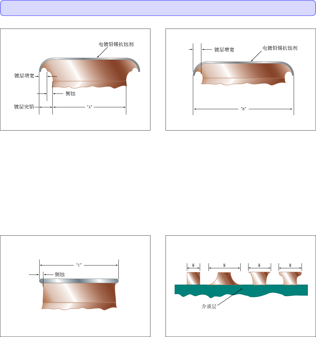
Note: The extent of outgrowth, if present, is related to the dry film resist thickness. Outgrowth occurs when the plating thickness exceeds
the resist thickness.
Note: The different etch configurations may not meet intended design requirements.
注: 镀层增宽的程度与干膜抗蚀剂的厚度有关。当镀层厚度超过抗蚀剂厚度时,就会产生镀层增宽。
注: 由于蚀刻外形的不同可能不能满足设计目的要求。
图321f
具有镀层增宽的图形电镀(干膜抗蚀剂)
图321h
具有镀层增宽的图形电镀(液态抗蚀剂)
图321g
薄铜箔与图形电镀(抗蚀剂)
图321i
随着表面阻剂W的不同,导体有效宽度与导体的宽度可能会不相同
3.2 CONDUCTIVE PATTERNS – GENERAL(导电图形 – 总则)
3.2.1 Etching Characteristics (cont.)(蚀刻特性(续))
95IPC-A-600H-2010 2010年4月
Visual observations made on cross-sections only.(仅对显微切片进行目检观察。)
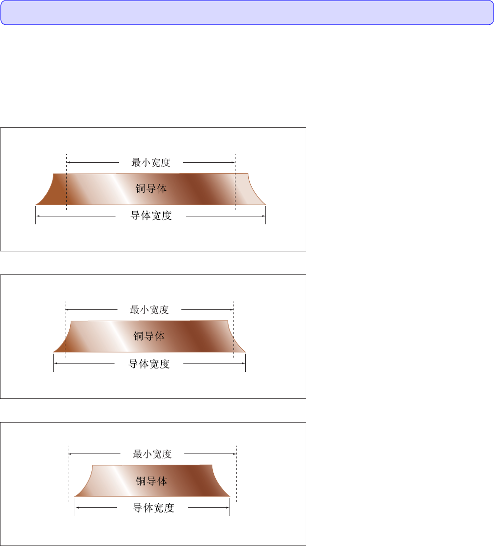
The copper conductor may consist of combinations of copper foil, copper plating and electroless copper. Metal resist, solder coatings, and
reflowed tin-lead plating that would normally be seen in a microsection are not shown in these illustrations.
铜导体可由铜箔、铜镀层及化学沉铜层组合而成。通常在显微切片中可以看到的金属抗蚀层、焊料涂覆层及热熔锡铅镀层,在这
里没有给出图示。
Target Condition - Class 1,2,3
(⽬标条件 - 1,2,3级)
• Conductor width exceeds minimum require-
ment.
• 导体宽度大于最小宽度要求。
Acceptable - Class 1,2,3
(可接受条件 - 1,2,3级)
• Conductor width meets minimum require-
ment.
• 导体宽度满足最小宽度要求。
Nonconforming - Class 1,2,3
(不符合条件 - 1,2,3级)
• Defects either do not meet or exceed above
criteria.
• 缺陷不符合或超出上述要求。
图322a
图322b
图322c
3.2 CONDUCTIVE PATTERNS – GENERAL(导电图形 – 总则)
3.2.2 Print and Etch(丝印及蚀刻)
96 IPC-A-600H-20102010年4月
Visual observations made on cross-sections only.(仅对显微切片进行目检观察。)