IPC-A-600H-2010 中文版 印制板的可接受性 (1).pdf - 第59页
Acceptable - Class 1 (可接受条件 - 1级) • Characters are legible. • Ink may be built up outside the character line providing the char- acter is legible. • Portion of component clocking symbol outline in the Figure 282c example…
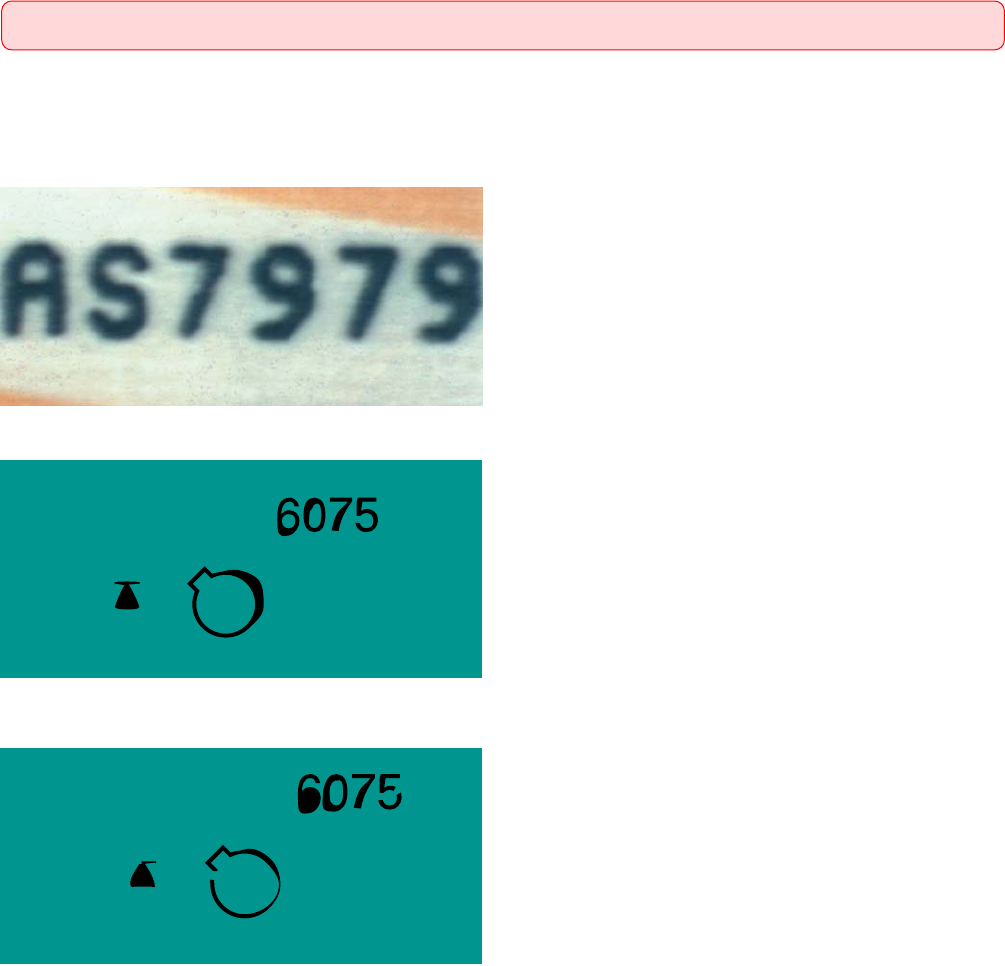
Screened or ink stamped marking refers to any type of marking that is printed on top of the printed board. No cutting or etching is involved
in producing this type of marking.
网印或油墨盖印标记指印在印制板面上的任何类型的标记。这种类型标记的制作不可含有切入或蚀刻的作法。
Target Condition - Class 1,2,3(⽬标条件 - 1,2,3级)
• Characters are legible.
• Ink distribution is uniform, with no smearing or double images.
• Ink markings are no closer than tangent to a land.
• 字符清晰可辨。
• 油墨分布均匀,没有模糊不清或重影。
• 油墨标记至多与焊盘相切。
Acceptable - Class 2,3(可接受条件 - 2,3级)
• Characters are legible.
• Ink may be built up outside the character line providing the char-
acter is legible.
• Portion of component clocking symbol outline in the Figure 282c
example may be missing, providing the required clocking is
clearly defined.
• Marking ink on component hole land does not extend into the part
mounting hole, or reduce minimum annular ring.
• Marking ink is allowed in PTHs and via holes into which no com-
ponent lead is soldered unless the procurement document requires
that the holes be completely solder filled.
• No encroachment of marking ink on edge board printed contacts
or test points.
• On surface mount lands with a pitch of 1.25 mm [0.04921 in] or
greater, encroachment of marking ink is on one side of land only
and does not exceed 0.05 mm [0.0020 in].
• On surface mount lands with a pitch less than 1.25 mm [0.04921
in], encroachment of marking ink is on one side of land only and
does not exceed 0.025 mm [0.000984 in].
• 字符清晰可辨。
• 只要字符可辨,油墨可以堆积在字符线条以外。
• 只要要求的方位仍清楚明确,图282c示例中所图示的元器件
方位符号的轮廓可以部分脱落。
• 元器件孔焊盘的标记油墨不得渗入部件安装孔内,或造成环
宽低于最小环宽。
• 除非采购文件要求孔被焊料完全填充,不焊接元器件引线的
镀覆孔和导通孔内允许有标记油墨。
• 阻焊剂没有侵占到板边印制接触片或测试点表面。
• 对于节距大于等于1.25mm[0.04921in]的表面贴装焊盘,油墨
只能侵占焊盘的一侧,且不超过0.05mm[0.0020in]。
• 对于节距小于1.25mm[0.04921in]的表面贴装焊盘,油墨只能
侵占焊盘的一侧,且不超过0.025mm[0.000984in]。
图282a
图282b
图282c
2.8 MARKING(标记)
2.8.2 Screened or Ink Stamped Marking(⽹印或油墨盖印标记)
50 IPC-A-600H-20102010年4月
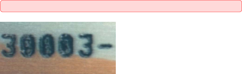
Acceptable - Class 1(可接受条件 - 1级)
• Characters are legible.
• Ink may be built up outside the character line providing the char-
acter is legible.
• Portion of component clocking symbol outline in the Figure 282c
example may be missing, providing the required clocking is
clearly defined.
• Marking ink on component hole land does not extend into the part
mounting hole, or reduce minimum annular ring.
• Marking ink is allowed in PTHs and via holes into which no com-
ponent lead is soldered unless the procurement document requires
that the holes be completely solder filled.
• No encroachment of marking ink on edge board printed contacts
or test points.
• On surface mount lands with a pitch of 1.25 mm [0.04921 in] or
greater, encroachment of marking ink is on one side of land only
and does not exceed 0.05 mm [0.0020 in].
• On surface mount lands with a pitch less than 1.25 mm [0.04921
in], encroachment of marking ink is on one side of land only and
does not exceed 0.025 mm [0.000984 in].
• Marking may be smeared or blurred provided it is still legible.
• Double images are legible.
• 字符清晰可辨。
• 只要字符可辨,油墨可以堆积在字符线条以外。
• 只要要求的方位仍清楚明确,图282c示例中所图示的元器件
方位符号的轮廓可以部分脱落。
• 元器件孔焊盘的标记油墨不得渗入部件安装孔内,或造成环
宽低于最小环宽。
• 除非采购文件要求孔被焊料完全填充,不焊接元器件引线的
镀覆孔和导通孔内允许有标记油墨。
• 阻焊剂没侵占到板边印制接触片或测试点表面。
• 对于节距大于等于1.25mm[0.04921in]的表面贴装焊盘,油墨
只能侵占焊盘的一侧,且不超过0.05mm[0.0020in]。
• 对于节距小于1.25mm[0.04921
in]的表面贴装焊盘,油墨只
能侵占焊盘的一侧,且不超过0.025mm[0.000984in]。
• 标记被涂污或模糊,但仍可辨认。
• 出现重影,但仍可辨认。
Nonconforming - Class 1,2,3(不符合条件 - 1,2,3级)
• Defects either do not meet or exceed above criteria.
• 缺陷不符合或超出上述要求。
图282d
2.8 MARKING(标记)
2.8.2 Screened or Ink Stamped Marking (cont.)(⽹印或油墨盖印标记(续))
51IPC-A-600H-2010 2010年4月

The term ‘‘Solder Mask’’ is used in this document as a general term when referring to any type of permanent polymer coating material used
on printed boards. Solder masks are used to limit and control the application of solder to selected areas of the printed board during assembly
soldering operations. Solder mask coatings are used to control and limit surface contamination of printed board surfaces during soldering and
subsequent processing operations, and are sometimes used to reduce dendritic filament growth(s) between conductive patterns over the
printed board base material surface. Detailed specifications and information regarding solder mask requirements are contained in IPC-6012
and IPC-SM-840.
Solder mask materials are not intended for use as a substitute for conformal coatings that are applied after assembly to cover components,
component lead/terminations and solder connections. Determination of compatibility of solder mask materials with conformal coating mate-
rials, or other substances, is dependent upon the end item assembly environments.
Solder mask thickness cannot be visually determined. If solder mask thickness is specified, microsectional analysis is required and evaluated
per 3.3.12.
The types of solder mask include:
• Deposited image, (liquid) screen printed form.
• Deposited image, electrostatic.
• Photo defined image, (liquid) form.
• Photo defined image, (dry film) form.
• Photo defined image, temporary mask.
• Photo defined, dry film over liquid.
Note: Touch up, if required to cover these areas with solder mask, shall be of a material that is compatible to and of equal resistance to sol-
dering and cleaning as the originally applied mask.
本文件使用的术语“阻焊膜(阻焊剂)”是指在印制板上用到的任何类型的永久性聚合物涂覆材料的通用术语。在装配焊接操作
期间,阻焊膜(阻焊剂)用来在印制板所选定的区域内限制及控制焊料的施加。阻焊涂覆层还用于在焊接中及后续的工艺操作中
控制及减少印制板表面的污染,有时还用于减少在印制板基材表面导电图形之间枝状细丝(枝晶)的生长。有关阻焊膜要求的详
细规范及信息参见IPC-6012和IPC-SM-840。
阻焊剂材料不能作为装配后覆盖元器件、元器件引线/端子及焊接连接的敷形涂覆层的代用品。阻焊剂材料与敷形涂覆材料或其
它材料兼容性的确定取决于最后组件的使用环境。
阻焊膜厚度不能通过目视检查确定。如果阻焊膜厚度有规定,则要求按3.3.12节做显微切片分析和评定。
阻焊剂的类型包括:
• 液态网印成像型;
• 静电沉积成像型;
• 液态光致成像型阻焊剂;
• 干膜光致成像型阻焊剂;
• 光致成像型暂性阻焊剂;
• 干膜覆盖在湿膜上的光致成像型阻焊剂。
注:如要求用阻焊膜修补以覆盖这些区域时,应当使用与最初使用的阻焊剂相兼容的并具有同等耐焊接性和耐清洗性的材料。
2.9 SOLDER MASK(阻焊膜(阻焊剂))
Introduction(引⾔)
52 IPC-A-600H-20102010年4月