IPC-A-600H-2010 中文版 印制板的可接受性 (1).pdf - 第73页
Nonconforming - Class 1,2,3 (不符合条件 - 1,2,3级) • Defects either do not meet or exceed above criteria. • 缺陷不符合或 超 出上述要求。 图 298e 图 298f 2.9 SOLDER MASK (阻焊膜(阻焊剂) ) 2.9.8 Soda Strawing (cont.) ( 吸管 状空 隙 (续) ) 65 IPC-A-600H-20…
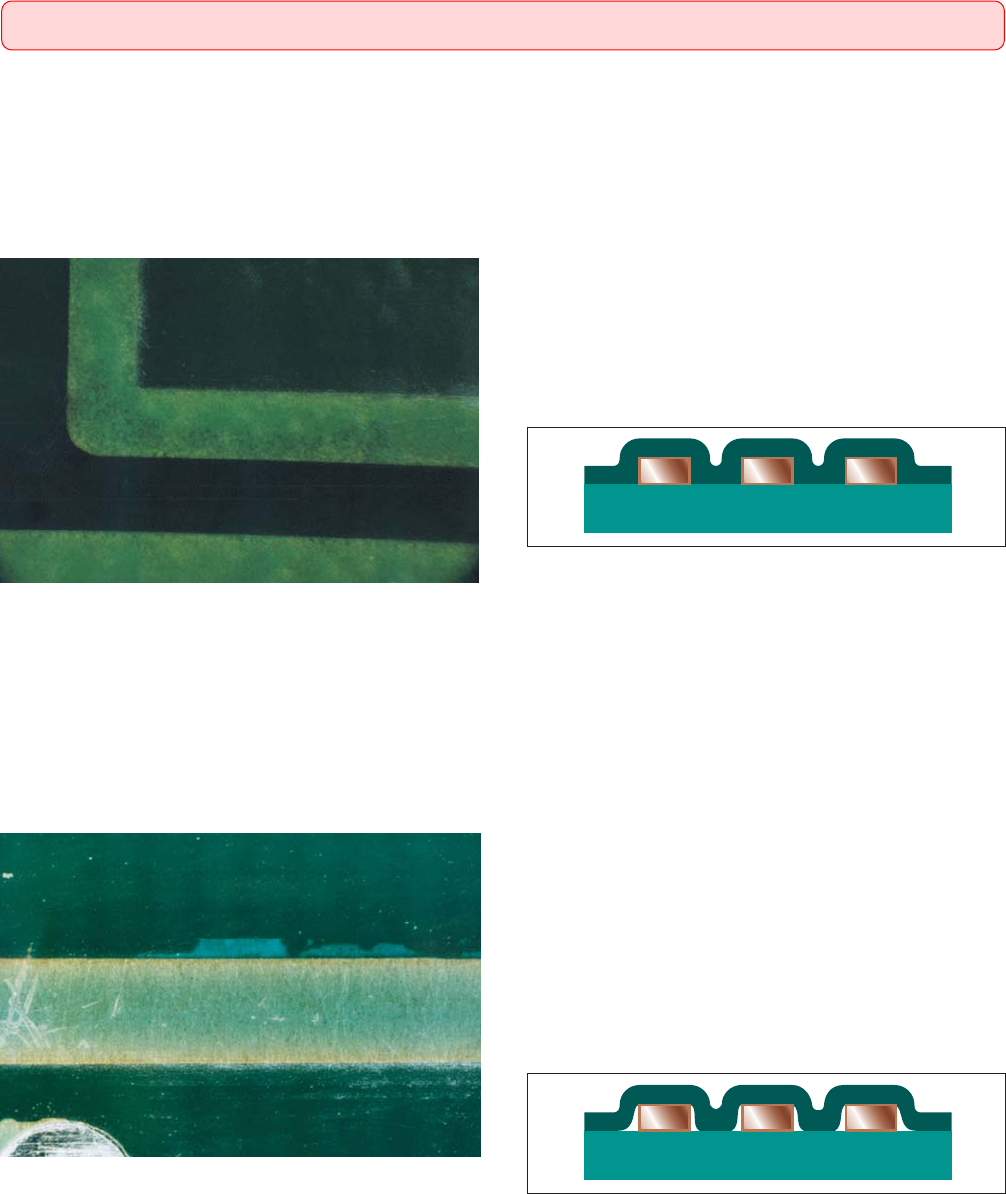
Soda Strawing: A long tubular-like void along the edges of conductive patterns where the solder mask is not bonded to the base material
surface or the edge of the conductor. Tin/lead fusing fluxes, fusing oils, solder fluxes, cleaning agents or volatile materials may be trapped in
the soda straw void.
吸管状空隙:沿着导电图形边缘的一种细长管状的空隙,即阻焊膜未与基材表面或导体边缘粘结。锡铅热熔助焊剂、热熔油、焊
接助焊剂、清洗剂或挥发物可能会被夹封在这种吸管状空隙中。
Target Condition - Class 1,2,3(⽬标条件 - 1,2,3级)
• No visible soda straw voids between the solder mask and the
printed board base material surface and the edges of the conduc-
tive patterns.
• 阻焊膜和印制板基材表面以及导电图形的侧边之间均不存在
可见空隙。
Acceptable - Class 3(可接受条件 - 3级)
• No evidence of soda strawing.
• 无吸管装空隙迹象。
Acceptable - Class 1,2(可接受条件 - 1,2级)
• Soda strawing along side conductive pattern edges does not
reduce the conductor spacing below the minimum requirements.
• Soda strawing is completely sealed from the external environ-
ment.
• 沿着导电图形侧面边缘出现吸管状空隙,但未使导体间距减
小至低于最小要求。
• 吸管状空隙与周围环境完全封闭。
图298a
图298c
图298b
图298d
2.9 SOLDER MASK(阻焊膜(阻焊剂))
2.9.8 Soda Strawing(吸管状空隙)
64 IPC-A-600H-20102010年4月
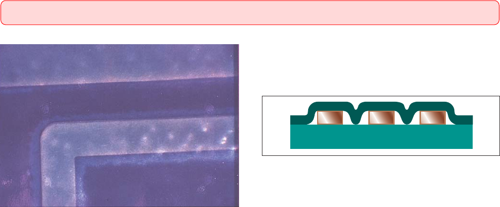
Nonconforming - Class 1,2,3(不符合条件 - 1,2,3级)
• Defects either do not meet or exceed above criteria.
• 缺陷不符合或超出上述要求。
图298e
图298f
2.9 SOLDER MASK(阻焊膜(阻焊剂))
2.9.8 Soda Strawing (cont.)(吸管状空隙(续))
65IPC-A-600H-2010 2010年4月

Printed boards shall meet the dimensional requirements specified on the procurement documentation such as printed board periphery, thick-
ness, cutouts, slots, notches and printed board edge contacts. The accuracy, repeatability and reproducibility of the equipment used to verify
the characteristics of printed boards should be 10% or less of the tolerance range of the dimensions being verified.
印制板应当满足采购文件规定的尺寸要求,如板的周边、厚度、切口、开槽、缺口及印制板边接触片等。用于验证印制板这些特
性的设备的精度、可重复性及可再现性应该为所验证尺寸公差范围的10%或更小。
2.10.1 Conductor Width and Spacing(导体宽度和间距)
This section covers acceptability requirements and criteria for conductor width and spacing. Acceptable conductor width and spacing is a
measure of how well the printed board fabrication process is reproducing the master image, which basically determines the width and spac-
ing requirements for the conductive patterns. Unless these characteristics are violated, edge definition itself is not necessarily a characteris-
tic for acceptance or nonconformance; however, it can be considered a process indicator, requiring review of manufacturing procedures. In
addition it may be an important consideration for controlled impedance circuits. Procurement documentation should establish edge definition
requirements for applications of these types. When required, measurements of conductor edge definition are made in accordance with IPC-
TM-650, Method 2.2.2.
本节包括导体宽度和间距的可接受性要求及准则。导体宽度和间距的可接受性是印制板制造工艺复现原始底片好坏的一种度量,
原始底片 已基本上确定了导电图形的最小宽度和间距要求。除非违反了这些特征,导体边缘的精确度不必作为验收或拒收的特
性,但却可作为一种制程警示,要求对生产工艺作出审核。此外,对控制阻抗电路,可能是一项需要考虑的重要因素。此类用途
的印制板应该在采购文件中规定边缘精确度要求。有要求时,按IPC-TM-650测试方法2.2.2测量导体边缘精确度。
2.10 PATTERN DEFINITION – DIMENSIONAL(图形精确度 – 尺⼨要求)
Introduction(引⾔)
66 IPC-A-600H-20102010年4月