IPC-A-600H-2010 中文版 印制板的可接受性 (1).pdf - 第96页
Minimum dielectric thickness is the maximum material condition used for the electrical voltage dielectric strength requirements. 最 小 介 质 厚 度 是 耐 电 压介 质强 度 要求的最大材料条件。 T arget Condition - Class 1,2,3 (⽬标条件 - 1,2,3级) • The …
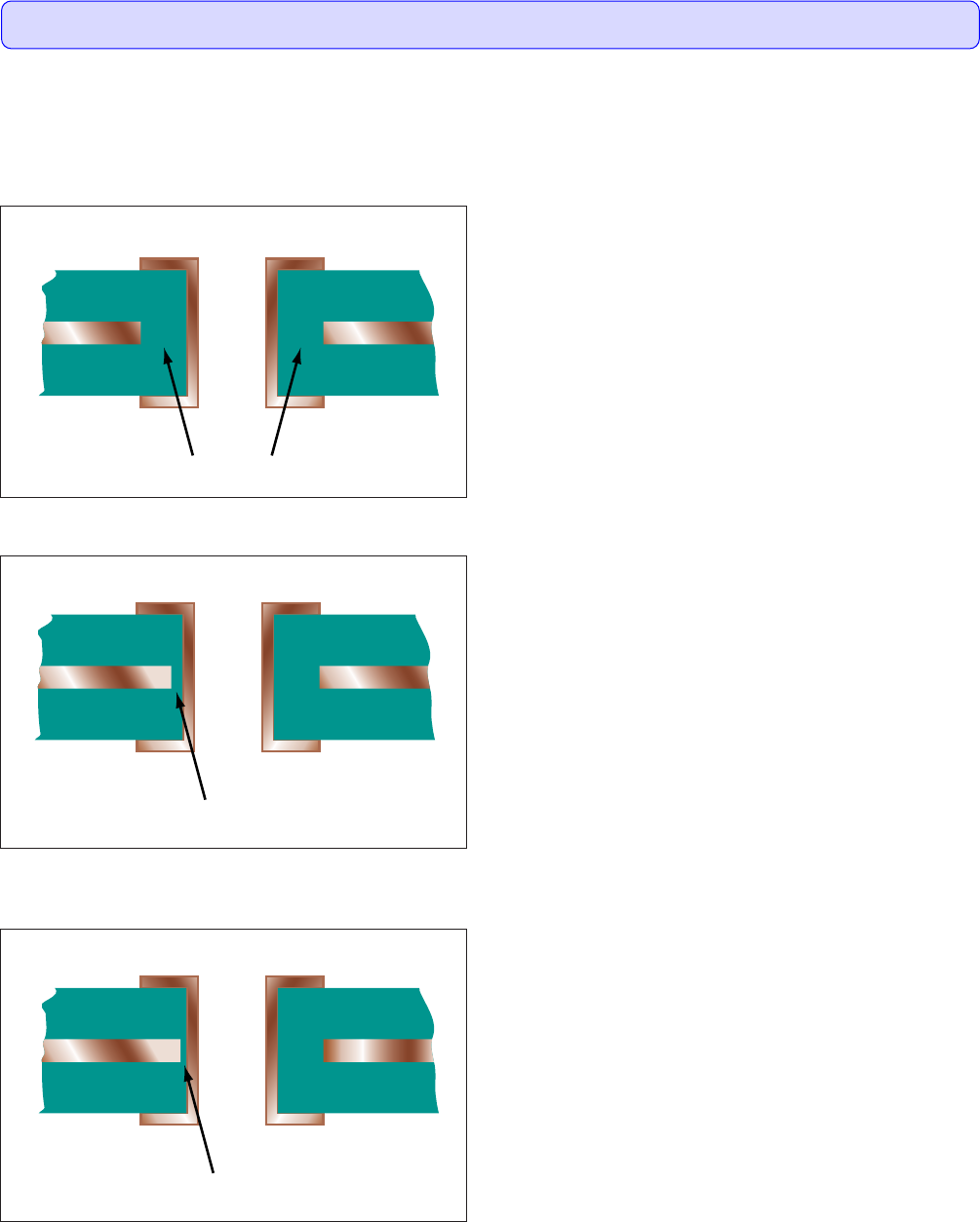
Metal planes are used for mechanical reinforcement and/or electromagnetic shielding for printed boards. Many requirements are the same as
for metal-core printed boards.
金属层用作印制板机械增强和(或)电磁屏蔽层,很多要求与金属芯印制板相同。
Target Condition - Class 1,2,3(⽬标条件 - 1,2,3级)
• Metal plane setback exceeds the procurement documentation
requirements.
• 金属层的余隙大于采购文件的要求。
Acceptable - Class 1,2,3(可接受条件 - 1,2,3级)
• Metal plane setback is equal to or greater than 0.1 mm [0.0040 in]
(when a value is not specified by the procurement documenta-
tion).
• Metal plane setback does not reduce the conductor spacing to less
than the specified minimum on the procurement documentation.
• 金属层的余隙等于或大于0.1mm[0.004in](当采购文件未给
出规定值时)。
• 金属层的余隙没有使导体间距减少到小于采购文件规定的最
小值。
Nonconforming - Class 1,2,3(不符合条件 - 1,2,3级)
• Defects either do not meet or exceed above criteria.
• 缺陷不符合或超出上述要求。
图317a
图317b
图317c
3.1 DIELECTRIC MATERIALS(介质材料)
3.1.7 Dielectric Material, Clearance, Metal Plane for Supported Holes(⾦属层上⽀撑孔的介质间距)
87IPC-A-600H-2010 2010年4月
Visual observations made on cross-sections only.(仅对显微切片进行目检观察。)
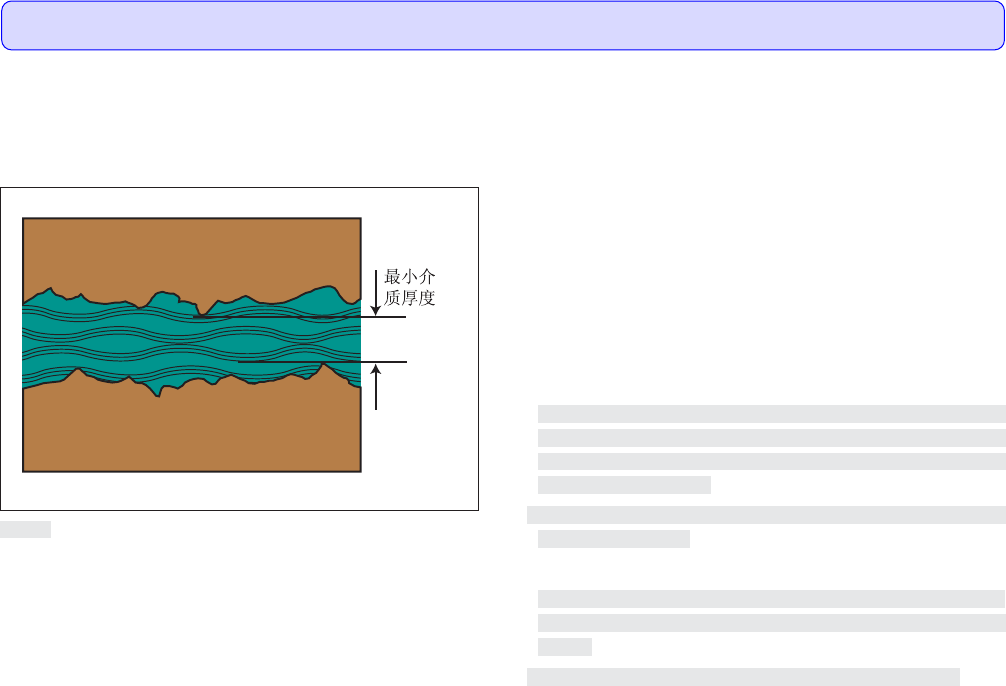
Minimum dielectric thickness is the maximum material condition used for the electrical voltage dielectric strength requirements.
最小介质厚度是耐电压介质强度要求的最大材料条件。
Target Condition - Class 1,2,3(⽬标条件 - 1,2,3级)
• The minimum dielectric thickness meets the requirements of the
procurement documentation.
• 最小介质厚度满足采购文件的要求。
Acceptable - Class 1,2,3(可接受条件 - 1,2,3级)
• The minimum dielectric thickness meets the minimum require-
ments of the procurement documentation.
• If the minimum dielectric spacing and the number of reinforcing
layers are not specified, the minimum dielectric spacing shall be
0.09 mm [0.0035 in] and the number of reinforcing layers shall be
selected by the supplier.
• Low profile copper foils should be used with dielectrics below
0.09 mm [0.0035 in].
• 最小介质厚度满足采购文件的最低要求。
• 如果最小介质间距和增强层的层数未作规定,则最小介质间
距应当为0.09mm[0.0035in],且增强层的层数应当由供应商
选择。
• 应该使用介质低于0.09mm[0.0035in]的低粗糙度铜箔。
Nonconforming - Class 1,2,3(不符合条件 - 1,2,3级)
• Defects either do not meet or exceed above criteria.
• 缺陷不符合或超出上述要求。
Notes:
1: Products designed for transmission line impedance applications may have special requirements and measurement method specified on
procurement documentation.
2: When the nominal dielectric thickness on the drawing is less than 90 µm [3,543 µin], the minimum dielectric spacing is 25 µm [984 µin]
and the number of reinforcing layers may be selected by the supplier.
注:
1. 为传输线阻抗应用而设计的产品,可在采购文件中规定特殊要求和测量方法。
2. 当图纸上的标称介质厚度小于90μm[3543μin]时,则最小介质间距为25μm[984μin],而增强层的层数可以由供应商选择。
图318a
3.1 DIELECTRIC MATERIALS(介质材料)
3.1.8 Layer-to-Layer Spacing(层间间距)
88 IPC-A-600H-20102010年4月
Visual observations made on cross-sections only.(仅对显微切片进行目检观察。)
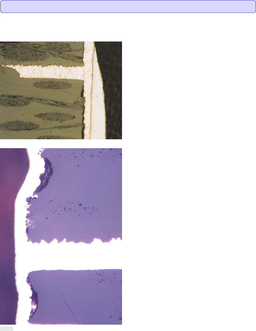
Resin Recession: A separation between the plated barrel of the hole and the dielectric material on the hole wall.
树脂凹缩:孔壁镀层与孔壁的介质材料之间出现分离的现象。
Acceptable - Class 1,2,3(可接受条件 - 1,2,3级)
• Resin recession is acceptable following thermal stress testing.
• 热应力测试后的树脂凹缩是可接受的。
图319a
图319b
3.1 DIELECTRIC MATERIALS(介质材料)
3.1.9 Resin Recession(树脂凹缩)
89IPC-A-600H-2010 2010年4月
Visual observations made on cross-sections only.(仅对显微切片进行目检观察。)