IPC-A-600H-2010 中文版 印制板的可接受性 (1).pdf - 第48页
Nonconforming - Class 1,2,3 (不符合条件 - 1,2,3级) • Defects either do not meet or exceed above criteria. • 缺陷不符合或 超 出上述要求。 图 271c 2.7 PRINTED CONT ACTS (印制接触⽚) 2.7.1 Surface Plating – Plated Contacts (cont.) (表⾯镀层 – 电镀的接触⽚(续)…
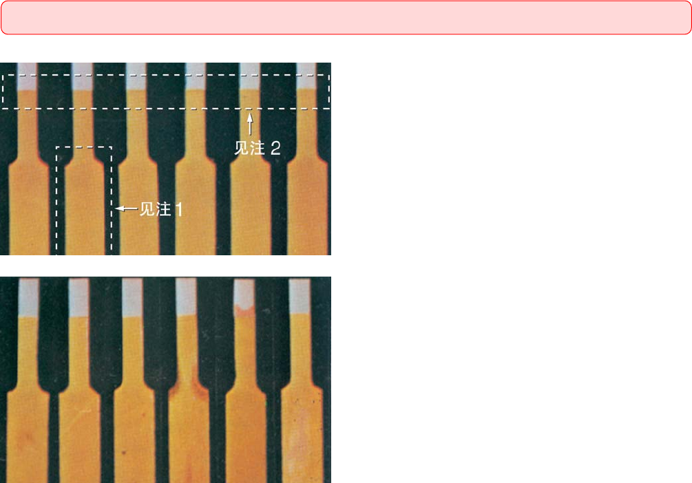
Target Condition - Class 1,2,3(⽬标条件 - 1,2,3级)
• Contacts are free of pits, pinholes and surface nodules.
• No exposed copper or plating overlap between solder finish or
solder mask and tip finish.
• 接触片上没有麻点、针孔和表面结瘤。
• 焊料涂覆层或阻焊膜与接触片末端涂覆层之间既没有露铜也
没有涂层重叠。
Acceptable - Class - 1,2,3 (Critical Contact Area)
(可接受条件 - 1,2,3级(关键接触区))
• Surface defects do not expose underlying metal in critical contact
area.
• Solder splashes or tin-lead plating does not occur in critical con-
tact area.
• No nodules and metal bumps in critical contact area.
• Pits, dents or depressions do not exceed 0.15 mm [0.00591 in] in
their longest dimension. There are not more than three per con-
tact, and they do not appear on more than 30% of the contacts.
• 在接插关键区内表面缺陷没有曝露底层金属。
• 在接插关键区内没有溅出的焊料或锡铅镀层。
• 在接插关键区内没有结瘤和金属突出。
• 麻点、凹坑或凹陷处的最长尺寸不超过0.15mm[0.00591in]。
每个接触片上的缺陷不超过3处,且有这些缺陷的接触片不
超过接触片总数的30%。
Acceptable - Class 3 (Gap/Overlap Area)
(可接受条件 - 3级(露铜/重叠区域))
• Exposed copper or plating overlap is 0.8 mm [0.031 in] or less.
• 露铜/镀层重叠区小于等于0.8mm[0.031in]。
Acceptable - Class 2 (Gap/Overlap Area)
(可接受条件 - 2级(露铜/重叠区域))
• Exposed copper or plating overlap does not exceed 1.25 mm
[0.04921 in].
• 露铜/镀层重叠区不超过1.25mm[0.04921in]。
Acceptable - Class 1 (Gap/Overlap Area)
(可接受条件 - 1级(露铜/重叠区域))
• Exposed copper or plating overlap does not exceed 2.5 mm
[0.0984 in].
• 露铜/镀层重叠区不超过2.5mm[0.0984in]。
Note 1: Discoloration is permitted in the plating overlap zone.
Note 2: Critical Contact Area. These conditions do not apply to a band 0.15 mm [0.00591 in] wide around the periphery of the printed con-
tact land.
注1:镀层重叠区允许变色。
注2:关键接插区域。这些条件不适用于围绕包括印制接触焊盘周围0.15mm[0.00591in]宽的区域。
图271a
图271b
2.7 PRINTED CONTACTS(印制接触⽚)
2.7.1 Surface Plating – Plated Contacts(表⾯镀层 – 电镀的接触⽚)
39IPC-A-600H-2010 2010年4月
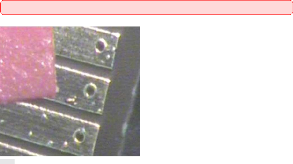
Nonconforming - Class 1,2,3(不符合条件 - 1,2,3级)
• Defects either do not meet or exceed above criteria.
• 缺陷不符合或超出上述要求。
图271c
2.7 PRINTED CONTACTS(印制接触⽚)
2.7.1 Surface Plating – Plated Contacts (cont.)(表⾯镀层 – 电镀的接触⽚(续))
40 IPC-A-600H-20102010年4月
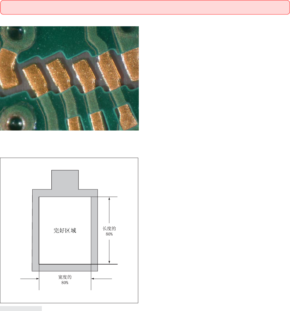
Target Condition - Class 1,2,3(⽬标条件 - 1,2,3级)
• Contacts are free of surface nodules, roughness, electrical test
witness marks or scratches that exceed 0.8 µm [32 µin] RMS
(root-mean-square) in the pristine area in accordance with an
applicable test method AABUS. If IPC-TM-650, Method 2.4.15,
is used, it is recommended that the roughness-width cutoff be
adjusted to approximately 80% of the maximum length of the
wire bond pad in order to obtain the RMS value within the pristine
area. For more information on surface roughness, refer to ASME
B46.1.
• The pristine area is defined as an area bounded in the center of the
pad by 80% of the pad width and 80% of the pad length (see Fig-
ure 2711b).
• 依据供需双方协商确定的测试方法测试后,接触片在完好区
域内没有超过0.8µm[32µin]RMS(均方根值)的表面结瘤、
粗糙、电气测试痕 记 或划痕。如使用IPC-TM-650测试方法
2.4.15,为了获得完好区域内的均方根值,建议把粗糙度截
除宽度调节至约为金属线键合盘最大长度的80%。关于表面
粗糙度的更多信息请参考ASME B46.1。
• 完好区域的定义是以引线键合盘中心为基准,引线键合盘长
度的80%和宽度的80%范围内的区域(见图2711b)。
图2711a
图2711b 完好区域
2.7 PRINTED CONTACTS(印制接触⽚)
2.7.1.1 Surface Plating – Wire Bond Pads(表⾯镀层 – ⾦属线键合盘)
41IPC-A-600H-2010 2010年4月