IPC-A-600H-2010 中文版 印制板的可接受性 (1).pdf - 第128页
T arget Condition - Class 1,2,3 (⽬标条件 - 1,2,3级) • No separation between the internal layer and plating in the hole. Direct bond of plated copper to layer foil copper. Line of demar- cation caused by preferential etching …
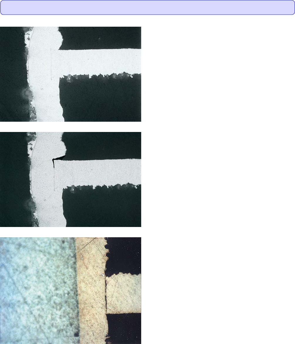
Target Condition - Class 1,2,3(⽬标条件 - 1,2,3级)
• Direct bond of plated copper to copper foil. No evidence of inner-
layer separation (separation between internal lands and plating of
the hole wall) or innerlayer inclusions.
• 镀铜层与铜箔直接接合,不存在内层分离(内层连接盘与孔
壁镀层间的分离)或内层夹杂物。
Acceptable - Class 2,3(可接受条件 - 2,3级)
• No separation evident.
• 没有分离迹象。
Acceptable - Class 1(可接受条件 - 1级)
• Partial innerlayer separation or innerlayer inclusions on only one
side of hole wall at each land location on no more than 20% of
each available land.
• 对于每个待钻孔焊盘,在不超过焊盘20%的范围内,只在孔
壁的一侧出现内层部分分离或内层夹杂物。
Nonconforming - Class 1,2,3(不符合条件 - 1,2,3级)
• Defects either do not meet or exceed above criteria.
• 缺陷不符合或超出上述要求。
图3314a
图3314b
图3314c
3.3 PLATED-THROUGH HOLES – GENERAL(镀覆孔 – 总则)
3.3.14 Innerlayer Separation – Vertical (Axial) Microsection(内层分离 – 垂直(轴向)显微切⽚)
119IPC-A-600H-2010 2010年4月
Visual observations made on cross-sections only.(仅对显微切片进行目检观察。)
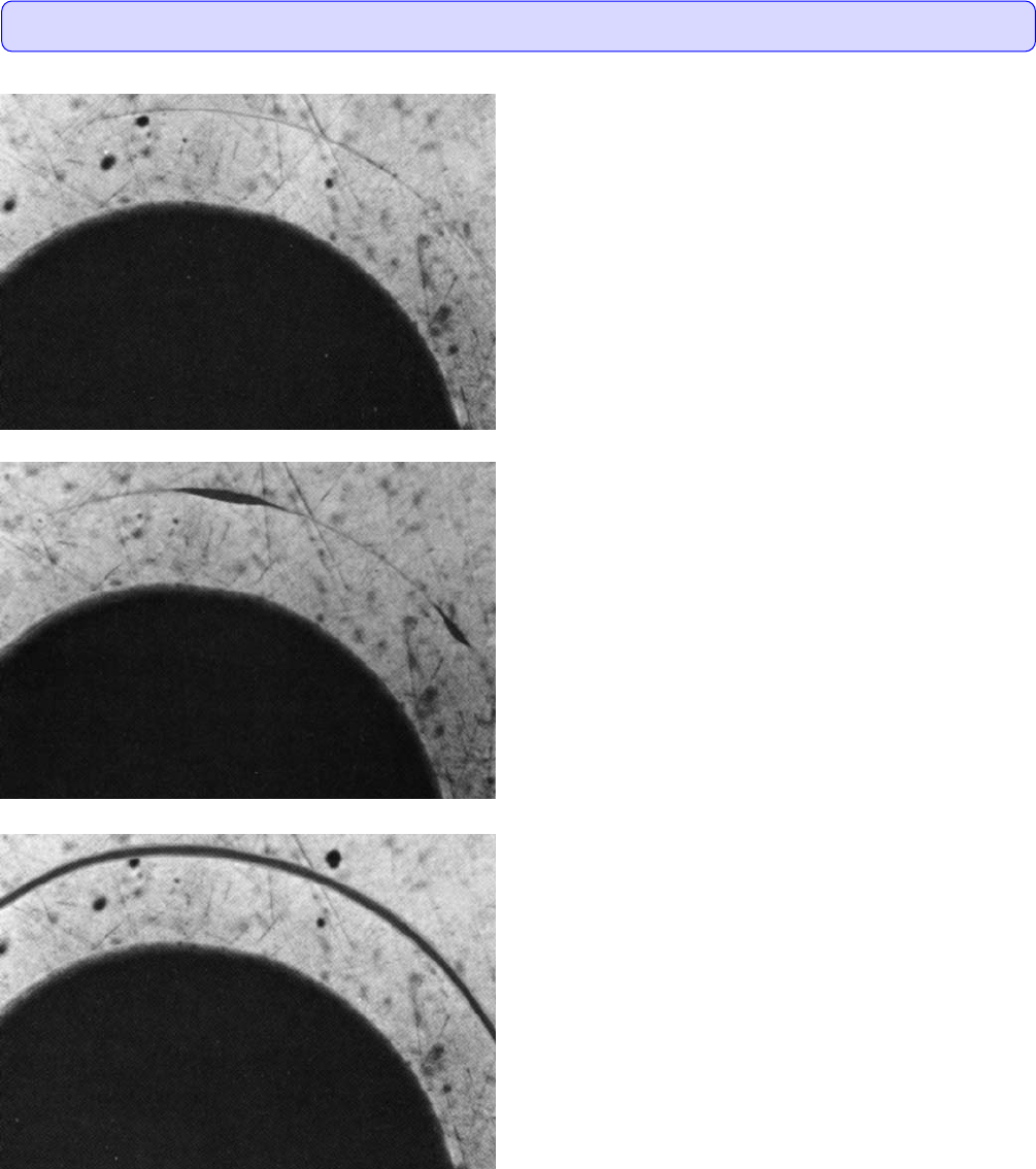
Target Condition - Class 1,2,3(⽬标条件 - 1,2,3级)
• No separation between the internal layer and plating in the hole.
Direct bond of plated copper to layer foil copper. Line of demar-
cation caused by preferential etching of electroless copper
deposit.
• 孔中内层铜箔与镀层之间没有分离。镀层与内层铜箔直接接
合,两者之间的分界线是由于化学镀铜优先蚀刻而形成的。
Acceptable - Class 2,3(可接受条件 - 2,3级)
• No separation evident.
• 没有分离迹象。
Acceptable - Class 1(可接受条件 - 1级)
• Slight line of demarcation and localized minor innerlayer separa-
tion that does not exceed specified requirements.
• 存在轻微的分界线并有轻微的局部内层分离,但尚未超过规
定的要求。
Nonconforming - Class 1,2,3(不符合条件 - 1,2,3级)
• Defects either do not meet or exceed above criteria.
• 缺陷不符合或超出上述要求。
图3315a
图3315b
图3315c
3.3 PLATED-THROUGH HOLES – GENERAL(镀覆孔 – 总则)
3.3.15 Innerlayer Separation – Horizontal (Transverse) Microsection(内层分离 – ⽔平(横向)显微切⽚)
120 IPC-A-600H-20102010年4月
Visual observations made on cross-sections only.(仅对显微切片进行目检观察。)
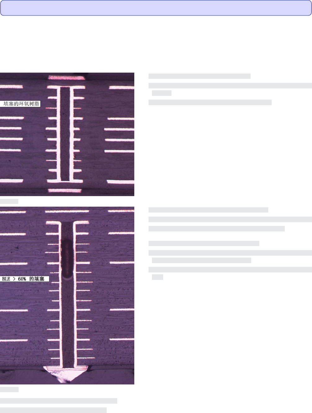
Blind via holes should be filled or plugged with a polymer or solder mask to prevent solder from entering them as solder in the small holes
tends to decrease reliability. Incomplete via fill may result in printed board delamination due to the rapid expansion of entrapped air pockets
or flux contaminants during solder reflow processes. Requirements for buried via fill are listed below.
盲导通孔应该用聚合物或阻焊剂填充或填塞以防止焊料进入,因为小孔内有焊料容易降低可靠性。孔未填满时,在再流焊过程
中,夹带的空气或助焊剂污染物会迅速膨胀而导致印制板分层。埋导通孔的填塞要求如下:
Target - Class 1,2,3(⽬标条件 - 1,2,3级)
• Complete fill of blind or buried via with laminating resin or similar fill
material.
• 盲/埋导通孔完全填满层压树脂或类似填塞材料。
Acceptable - Class 1,2,3(可接受条件 - 1,2,3级)
• At least 60% buried via fill with laminating resin or similar fill material.
• 层压树脂或类似填充材料至少填塞了埋导通孔的60%。
Acceptable - Class 2,3(可接受条件 - 2,3级)
• At least 60% fill for blind vias with an aspect ratio greater than 1:1 or as
specified in the procurement documentation.
• 厚径比大于1 : 1 的 盲 导通孔至少被填塞了60%或符合采购文件规
定。
Note: Through hole fill requirements are AABUS.
注: 通孔的填塞要求由供需双方协商确定。
图3316a
图3316b
3.3 PLATED-THROUGH HOLES – GENERAL(镀覆孔 – 总则)
3.3.16 Material Fill of Blind and Buried Vias(埋/盲导通孔的材料填塞)
121IPC-A-600H-2010 2010年4月
Visual observations made on cross-sections only.(仅对显微切片进行目检观察。)