IPC-A-600H-2010 中文版 印制板的可接受性 (1).pdf - 第105页
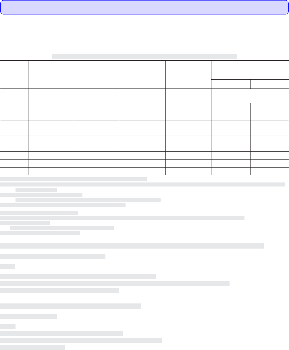
Unless otherwise specified on the procurement documentation, the minimum total (copper foil plus copper plating) conductor thickness after processing shall be in accordance with Table 3-1. 除 非 采 购 文件 另 有规定,加工 后 最 小总导 体 厚…
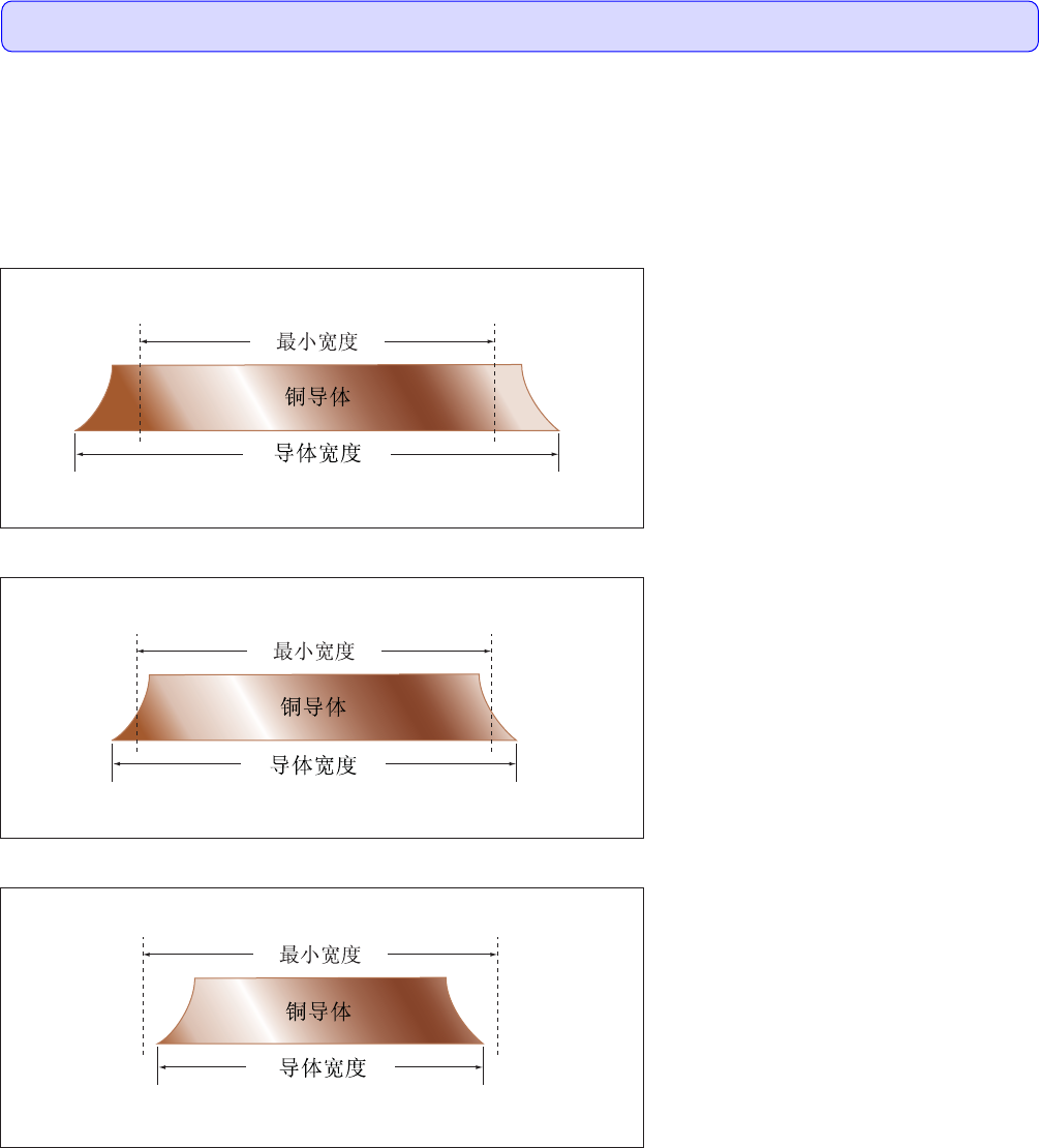
The copper conductor may consist of combinations of copper foil, copper plating and electroless copper. Metal resist, solder coatings, and
reflowed tin-lead plating that would normally be seen in a microsection are not shown in these illustrations.
铜导体可由铜箔、铜镀层及化学沉铜层组合而成。通常在显微切片中可以看到的金属抗蚀层、焊料涂覆层及热熔锡铅镀层,在这
里没有给出图示。
Target Condition - Class 1,2,3
(⽬标条件 - 1,2,3级)
• Conductor width exceeds minimum require-
ment.
• 导体宽度大于最小宽度要求。
Acceptable - Class 1,2,3
(可接受条件 - 1,2,3级)
• Conductor width meets minimum require-
ment.
• 导体宽度满足最小宽度要求。
Nonconforming - Class 1,2,3
(不符合条件 - 1,2,3级)
• Defects either do not meet or exceed above
criteria.
• 缺陷不符合或超出上述要求。
图322a
图322b
图322c
3.2 CONDUCTIVE PATTERNS – GENERAL(导电图形 – 总则)
3.2.2 Print and Etch(丝印及蚀刻)
96 IPC-A-600H-20102010年4月
Visual observations made on cross-sections only.(仅对显微切片进行目检观察。)
Unless otherwise specified on the procurement documentation, the minimum total (copper foil plus copper plating) conductor thickness after
processing shall be in accordance with Table 3-1.
除非采购文件另有规定,加工后最小总导体厚度(铜箔加上铜镀层)应当满足表3-1的规定:
Table 3-1 External Conductor Thickness after Plating(表3-1 电镀后外层导体厚度)
Weight
1,4
Absolute Cu Min.
(IPC-4562 less
10% reduction)
(µm) [µin]
Plus minimum
plating for
Class 1 and 2
(20 µm) [787 µin]
2
Plus minimum
plating for Class 3
(25 µm) [984 µin]
2
Maximum Variable
Processing
Allowance
Reduction
3
(µm) [µin]
Minimum Surface
Conductor Thickness after
Processing (µm) [µin]
Class1&2 Class3
重量
1,4
铜绝对最⼩值
(IPC-4562
规定值减10%)
(µm)[µin]
对于1级和2
级产品,
加上最⼩镀层
(20µm)[787µin]
2
对于3级产品,
加上最⼩镀层
(25µm)[984µin]
2
加⼯中允许
减少的最⼤值
(µm)[µin]
3
加⼯后的最⼩表⾯导体厚度
(µm)[µin]
1级和2级 3级
1/8 oz. 4.60 [181] 24.60 [967] 29.60 [1,165] 1.50 [59] 23.1 [909] 28.1 [1,106]
1/4 oz. 7.70 [303] 27.70 [1,091] 32.70 [1,287] 1.50 [59] 26.2 [1,031] 31.2 [1,228]
3/8 oz. 10.80 [425] 30.80 [1,213] 35.80 [1,409] 1.50 [59] 29.3 [1,154] 34.3 [1,350]
1/2 oz. 15.40 [606] 35.40 [1,394] 40.40 [1,591] 2.00 [79] 33.4 [1,315] 38.4 [1,512]
1 oz. 30.90 [1,217] 50.90 [2,004] 55.90 [2,201] 3.00 [118] 47.9 [1,886] 52.9 [2,083]
2 oz. 61.70 [2,429] 81.70 [3,217] 86.70 [3,413] 3.00 [118] 78.7 [3,098] 83.7 [3,295]
3 oz. 92.60 [3,646] 112.60 [4,433] 117.60 [4,630] 4.00 [157] 108.6 [4,276] 113.6 [4,472]
4 oz. 123.50 [4,862] 143.50 [5,650] 148.50 [5,846] 4.00 [157] 139.5 [5,492] 144.5 [5,689]
Note 1. Starting foil weight of design requirement per procurement documentation.
Note 2. Process allowance reduction does not allow for rework processes for weights below
1
⁄
2
oz. For
1
⁄
2
oz. and above, the process allowance reduction allows
for one rework process.
Note 3. Reference: Min. Cu Plating Thickness
Class1=20µm[787µin] Class2=20µm[787µin] Class3=25µm[984µin]
Note 4. For copper foil above 4 oz., utilize the formula provided below.
注1:采购文件中起始铜箔重量的设计要求。
注2:对于重量小于1/2oz的铜箔,加工减少厚度值不允许进行返工制程。对于1/2oz或以上的铜箔,加工减少厚度值允许进行一次返工制程。
注3:参考:最小铜镀层厚度
1级=20µm[787µin] 2级=20µm[787µin] 3级=25µm[984µin]
注4:对于大于4oz的铜箔,采用以下的公式。
The minimum surface conductor thickness after processing values given in Table 3-1 are determined by the following equation:
Minimum Surface Conductor Thickness=a+b-c
Where:
a = Absolute copper foil minimum (IPC-4562 nominal less 10% reduction).
b = Minimum copper plating thickness (20 µm [787 µin] for Class 1 and Class 2; 25 µm [984 µin] for Class 3).
c = A maximum variable processing allowance reduction.
表3-1中给出的加工后最小表面导体厚度的值由下列公式确定:
表面导体最小厚度= a+b-c
此处:
a=铜箔最小厚度绝对值(比IPC-4562标称值少10%)。
b=最小铜镀层厚度(1级和2级为20µm[787µin];3级为25µm[984µin])。
c=加工允许减少的最大值。
3.2 CONDUCTIVE PATTERNS – GENERAL(导电图形 – 总则)
3.2.3 Surface Conductor Thickness (Foil Plus Plating)(表⾯导体厚度(铜箔加上镀层))
97IPC-A-600H-2010 2010年4月
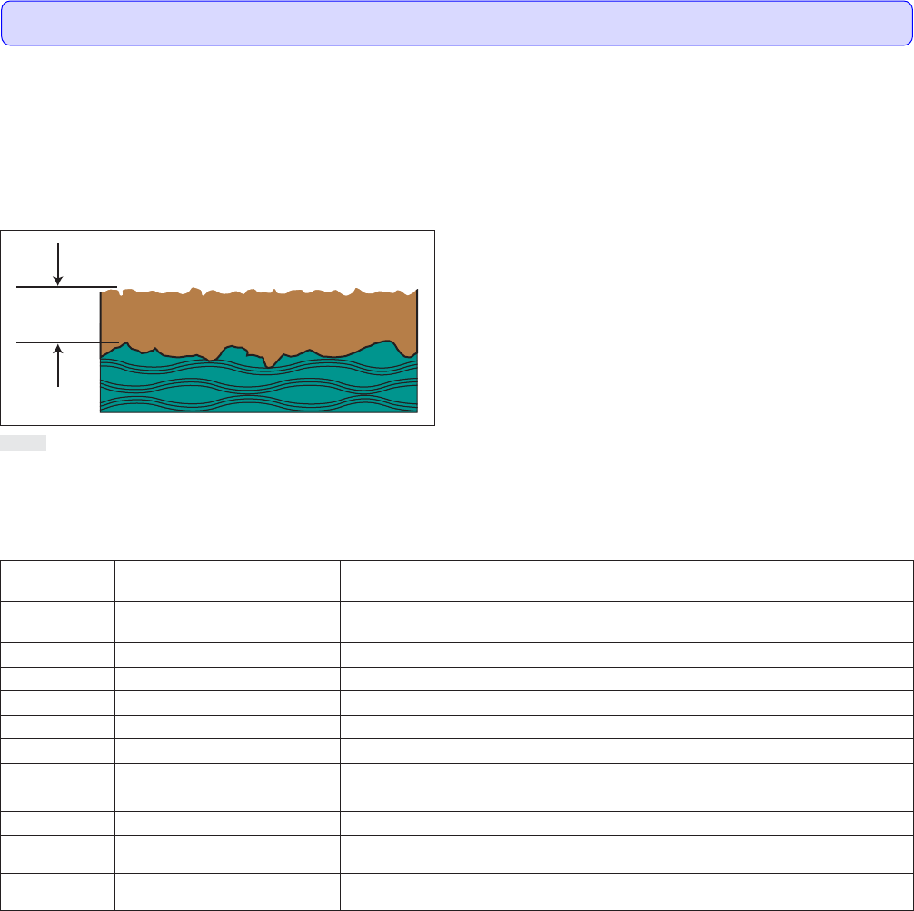
Minimum foil thickness (or conductor thickness) is the maximum continuous coplanar thickness that will conduct electrical current.
Individual scratches are included, but the saw-toothed shaped ‘‘dendritic’’ surface for metal-clad adhesion promotion is excluded from the
minimum foil thickness determination, as shown in Figure 324a.
最小铜箔厚度(或导体厚度)是传导电流的最大的连续共面厚度。
确定最小铜箔厚度时,包括个别的划痕,但用于加强金属箔粘结强度的锯齿状“树枝形”表面除外,如图324a所示。
The minimum internal layer foil thickness after processing shall be in accordance with Table 3-2.
加工后所有级别产品的最小内层铜箔厚度应当符合表3-2的规定:
Table 3-2 Internal Layer Foil Thickness after Processing
Weight
Absolute Cu Min. (IPC-4562
less 10% reduction) (µm) [µin]
Maximum Variable Processing
Allowance Reduction
1
(µm) [µin]
Minimum Final Finish
after Processing (µm) [µin]
重量
铜绝对最⼩值(⽐IPC-4562规定
值减少10%)(µm)[µin]
加⼯允许的最⼤减少量
1
(µm)[µin]
加⼯后成品导体最⼩厚度
(µm)[µin]
1/8 oz. [5.10] 4.60 [181] 1.50 [59] 3.1 [122]
1/4 oz. [8.50] 7.70 [303] 1.50 [59] 6.2 [244]
3/8 oz. [12.00] 10.80 [425] 1.50 [59] 9.3 [366]
1/2 oz. [17.10] 15.40 [606] 4.00 [157] 11.4 [449]
1 oz. [34.30] 30.90 [1,217] 6.00 [236] 24.9 [980]
2 oz. [68.60] 61.70 [2,429] 6.00 [236] 55.7 [2,193]
3 oz. [102.90] 92.60 [3,646] 6.00 [236] 86.6 [3,409]
4 oz. [137.20] 123.50 [4,862] 6.00 [236] 117.5 [4,626]
Above 4 oz.
[137.20]
IPC-4562 value
less 10% reduction
6.00 [236]
6 µm [236 µin] below minimum thickness of calcu-
lated 10% reduction of foil thickness in IPC-4562
4oz. [137.20]
以上
比IPC-4562规定值减少10% 6.00 [236]
比根据IPC-4562规定值减少10%
计算出的最小厚度少6µm[236µin]
Note 1. Process allowance reduction does not allow for rework processes for weights below
1
⁄
2
oz. For
1
⁄
2
oz. and above, the process allowance reduction allows
for one rework process.
Note 2. Additional platings that may be required for internal layer conductors shall be separately designated as a plating thickness requirement.
注1:对于重量小于1/2oz的铜箔,加工减少厚度值不允许进行返工制程。对于1/2oz及其以上的铜箔,加工减少厚度值允许进行一次返工制程。
注2:内层导体需要额外镀层时,应当单独规定其镀层厚度。
图324a
3.2 CONDUCTIVE PATTERNS – GENERAL(导电图形 – 总则)
3.2.4 Foil Thickness – Internal Layers(内层铜箔厚度)
Visual observations made on cross-sections only.
98 IPC-A-600H-20102010年4月