IPC-A-600H-2010 中文版 印制板的可接受性 (1).pdf - 第109页
For multilayer printed boards, in addition to physical measurements of printed board surfaces, if internal annular ring breakout is detected in the vertical cross section, but the degree of breakout cannot be determined,…

Microsection:
• Plating thickness measurements
A. Encapsulated Microsection Examination (IPC-TM-650, Method 2.1.1 or Method 2.1.1.2): The average copper thickness should be
determined from three measurements, approximately equally spaced, on each side of the PTH. Do not measure in areas having isolated
imperfections such as voids, cracks or nodules. Small localized areas with plating thickness less than minimum requirement are evalu-
ated as voids.
B. Nondestructive Method: Micro-ohm Measurements (IPC-TM-650, Method 2.2.13.1): This technique may be used to measure the aver-
age copper thickness in PTH when properly standardized. The method has application to measurement of the minimum copper thick-
ness. Due to the dependence on uniform hole geometry this method may not be appropriate for measurement of punched PTHs. The
nondestructive feature and the speed and ease of measurement make this method useful in providing variable data for statistical process
control.
C. Plating Thickness: Minimum requirements are established in IPC-6010 series.
• Solderability
A lot sample or representative specimen should be subjected to a solderability test utilizing Methods B, B1, C, C1, D or D1 of IPC-J-STD-
003. The coating durability requirement should be pre-established. The PTHs should exhibit good wetting and capillary action.
显微切⽚:
• 镀层厚度测量
A. 灌封的显微切片检验(IPC-TM-650测试方法2.1.1或2.1.1.2):铜的平均厚度应该通过三个测量值来确定,在镀覆孔每侧壁
上大约等距离选取三个测试点。不要选用有孤立缺陷的区域,例如空洞、裂缝或结瘤等来测量镀铜厚度。小的局部区域镀
层厚度低于最小要求的,作为空洞来评定。
B. 非破坏性方法:微欧姆测量法(IPC-TM-650测试方法2.2.13.1):当此法经过适当的标定后,这种技术可用来测量镀覆孔铜
层的平均厚度。这种方法用来测量镀铜的最小厚度。由于此法与孔的形状的均匀性有关,因此不适合用于测定冲孔的镀覆
孔内的镀铜厚度。由于非破坏性的特点、快速且易于测量,使这种方法在为“统计过程控制”(SPC)提供计量数据时非
常有用。
C. 镀层厚度:IPC-6010系列标准建立了最小厚度要求。
• 可焊性
所选取的一批次具有代表性的样品应该采用ANSI/J-STD-003的B、B1、C、C1、D或D1测试方法进行可焊性测试。应该事先确
定涂覆层的耐久性要求。镀覆孔应该呈现良好的润湿和毛细作用。
3.3
PLA
TED-THROUGH HOLES – GENERAL(镀覆孔 – 总则)
Introduction (cont.)(引⾔(续))
100 IPC-A-600H-20102010年4月
For multilayer printed boards, in addition to physical measurements of printed board surfaces, if internal annular ring breakout is detected in
the vertical cross section, but the degree of breakout cannot be determined, internal registration may be assessed by nondestructive techniques
other than microsection, such as, special patterns, probes, and/or software, which are configured to provide information on the interpolated
annual ring remaining and pattern skew. Techniques include, but are not limited to the following:
• The optional F or R coupon detailed in IPC-2221.
• Custom designed electrically testable coupons.
• Radiographic (x-ray) techniques.
• Horizontal microsection.
• CAD/CAM data analysis as correlated to pattern skew by layer.
Note: Microsectioning or statistical sampling shall be used to verify correlation of the approved technique, and a calibration standard estab-
lished for the specific technique employed.
If misregistration to the point of breakout is detected in vertical microsections, the concerns are that:
1. The conductor width minimum may be compromised at the land junction and,
2. There is insufficient electrical spacing.
The extent and direction of breakout shall be determined. Appropriate test coupons or actual production printed boards shall be tested at the
affected area(s) and analyzed on the suspect layer(s) to determine compliance. This may be accomplished by the techniques listed above.
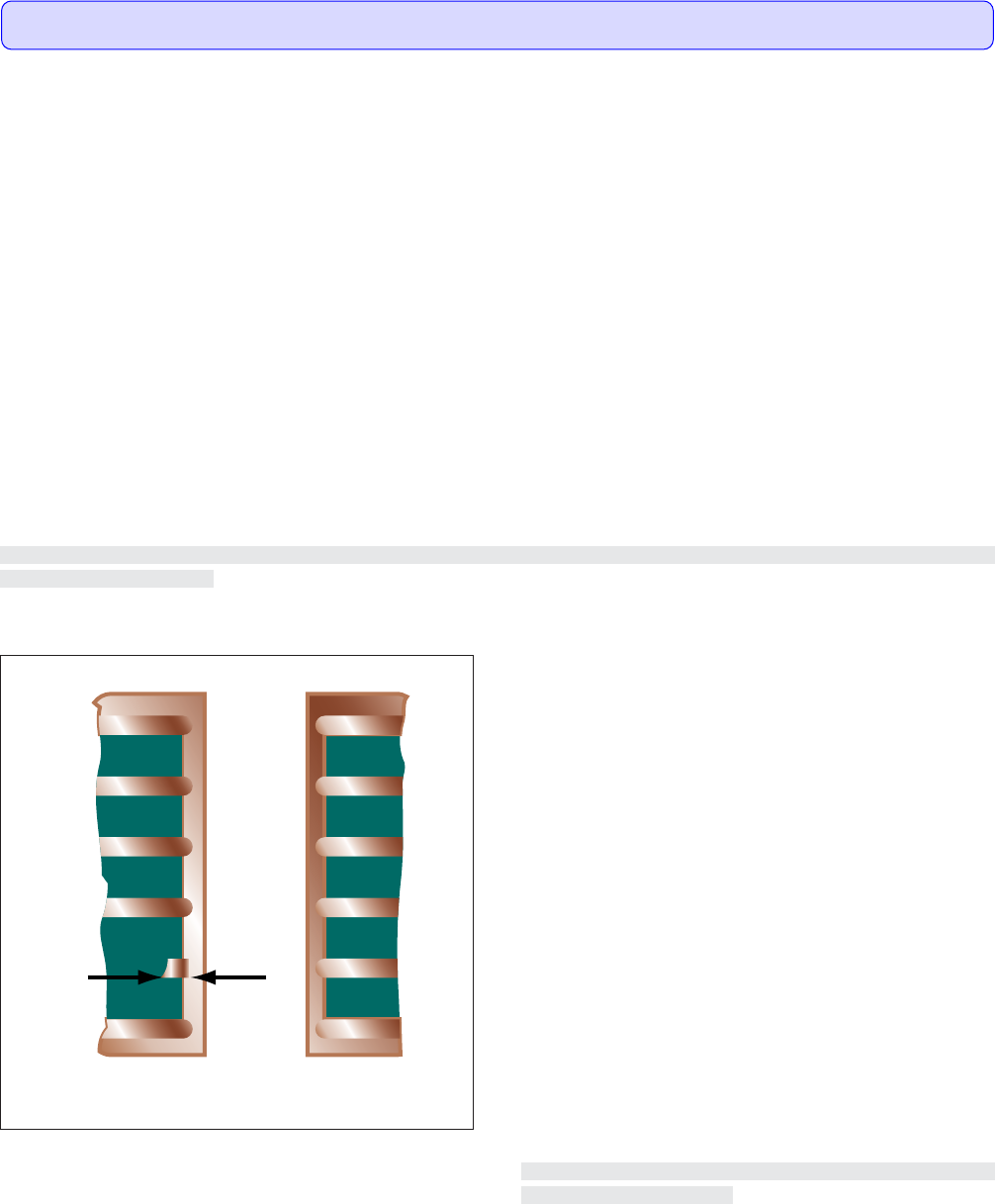
Measurements for internal annular ring are taken at the copper hole wall plating/internal land interface to the outer most tip of the internal
land as shown in Figure 331a.
对于多层印制板,除了要测量印制板表面特性之外,如在垂直
显微剖切中发现内层孔环有破环,但不能判定破环的程度,
内层的错位则可通过除显微剖切外的非破环性方法确定,例如
特殊图形、探头及(或)软件。其原理是利用错位的孔环和
偏斜的图形找到情况。这类技术包含但不局限于以下几种:
• IPC-2221中详细描述的可选附连板F或R;
• 定制的可用于电气测试的附连板;
•X射线术;
• 水平显微剖切;
• 与每层图形定位相关的CAD/CAM资料分析
注:应当采用显微剖切或统计抽样来验证上述检测技术的符
合性,及为所采用的具体技术建立的特定校准标准。
一旦在垂直显微切片上发现错位,注意下列事项:
1. 在导体与焊盘的连接区,最小导体宽度可能受到危及;
2. 没有足够的电气间距。
应当测定破环的大小与方向。应当在适用的测试附连板或实
际成品印制板的受影响区域进行测试,并分析可疑层面从而
进行判定。可通过以上所列的技术进行评定。
内层环宽的测量从孔壁的铜镀层/内部连接盘界面测至内部连
接盘的最外端,如图331a。
图331a
3.3 PLATED-THROUGH HOLES – GENERAL(镀覆孔 – 总则)
3.3.1 Annular Ring – Internal Layers(内层环宽)
101IPC-A-600H-2010 2010年4月
Visual observations made on cross-sections only.(仅对显微切片进行目检观察。)
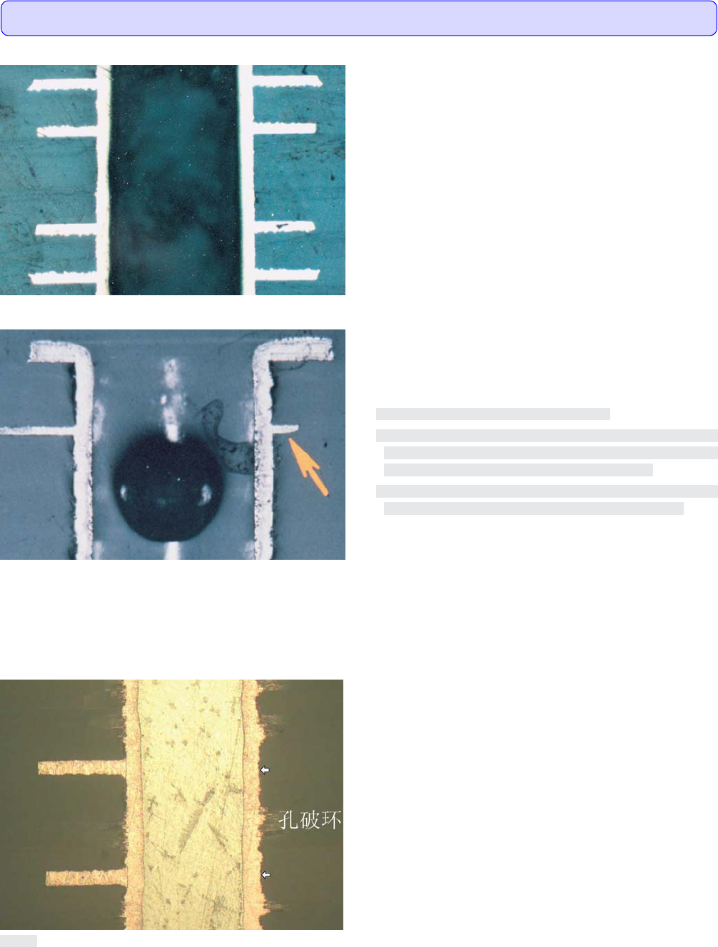
Target Condition - Class 1,2,3(⽬标条件 - 1,2,3级)
• All holes accurately registered in the center of the lands.
• 所有的孔准确地对准焊盘的中心。
Acceptable - Class 3(可接受条件 - 3级)
• Annular ring measures 0.025 mm [0.000984 in] or more.
• 环宽大于或等于0.025mm[0.000984in]。
Acceptable - Class 2(可接受条件 - 2级)
• 90° hole breakout is allowed provided the land/conductor junc-
tion is not reduced below the allowable width reduction in
2.10.1.1 and minimum lateral spacing is maintained.
• 如破环未使焊盘/导体连接区减少至小于2.10.1.1节允许的宽
度减少值并保持最小侧向间距,则允许有90°的破环。
Acceptable - Class 1(可接受条件 - 1级)
• Hole breakout is allowed provided the land/conductor junction is
not reduced below the allowable width reduction in 2.10.1.1 and
minimum lateral spacing is maintained.
• 如破环未使焊盘/导体连接区减少至小于2.10.1.1节允许的宽
度减少值并保持最小间距。
Nonconforming - Class 1,2,3(不符合条件 - 1,2,3级)
• Defects either do not meet or exceed above criteria.
• 缺陷不符合或超出上述要求。
图331d
图331c
图331b
3.3 PLATED-THROUGH HOLES – GENERAL(镀覆孔 – 总则)
3.3.1 Annular Ring – Internal Layers (cont.)(内层环宽(续))
102 IPC-A-600H-20102010年4月
Visual observations made on cross-sections only.(仅对显微切片进行目检观察。)