IPC-A-600H-2010 中文版 印制板的可接受性 (1).pdf - 第88页
T arget Condition - Class 1,2,3 (⽬标条件 - 1,2,3级) • No delamination or blistering. • 无 分 层 或起泡。 Acceptable - Class 2,3 (可接受条件 - 2,3级) • No evidence of delamination or blistering. • 没有分 层 或起泡 迹 象。 Acceptable - Class 1 (可接受条…
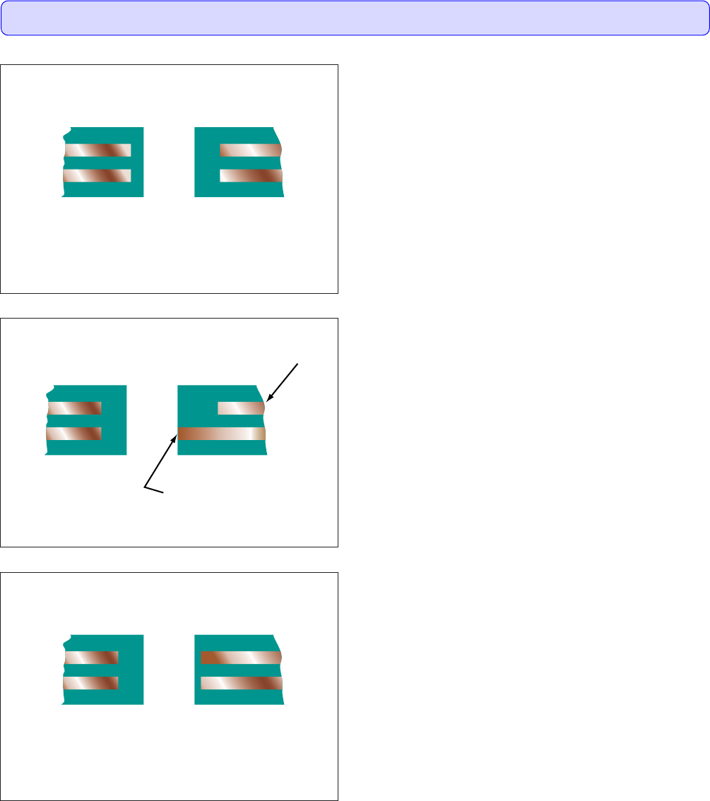
Target Condition - Class 1,2,3(⽬标条件 - 1,2,3级)
• Power/Ground plane setback meets the procurement documenta-
tion requirements.
• 电源层/接地层到隔离孔的余隙符合采购文件的要求。
Acceptable - Class 1,2,3(可接受条件 - 1,2,3级)
• A) Power/ground plane setback is greater than the minimum elec-
trical conductor spacing specified on the procurement documen-
tation.
• B) Ground plane may extend to the edge of an unsupported hole
when specified in the procurement documentation.
•A)电源层/接地层到隔离孔的余隙大于采购文件规定的最
小导体间距。
•B)当采购文件有规定时,接地层可以延伸到非支撑孔的边
缘。
Nonconforming - Class 1,2,3(不符合条件 - 1,2,3级)
• Defects either do not meet or exceed above criteria.
• 缺陷不符合或超出上述要求。
图313a
图313b
A
B
图313c
3.1 DIELECTRIC MATERIALS(介质材料)
3.1.3 Clearance Hole, Unsupported, to Power/Ground Planes(电源层/接地层上的⾮⽀撑孔,隔离孔)
79IPC-A-600H-2010 2010年4月
Visual observations made on cross-sections only.(仅对显微切片进行目检观察。)
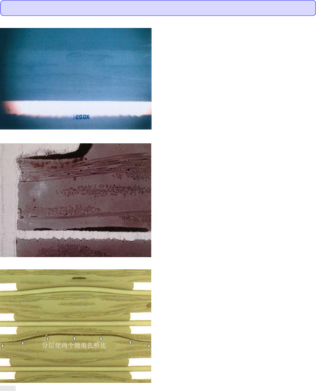
Target Condition - Class 1,2,3(⽬标条件 - 1,2,3级)
• No delamination or blistering.
• 无分层或起泡。
Acceptable - Class 2,3(可接受条件 - 2,3级)
• No evidence of delamination or blistering.
• 没有分层或起泡迹象。
Acceptable - Class 1(可接受条件 - 1级)
• If delamination or blistering is present, evaluate the entire printed
board in accordance with 2.3.3.
• 如出现分层或起泡,按2.3.3节的要求来评定整个印制板。
Nonconforming - Class 1,2,3(不符合条件 - 1,2,3级)
• Defects either do not meet or exceed above criteria.
• 缺陷不符合或超出上述要求。
图314a
图314b
图314c
3.1 DIELECTRIC MATERIALS(介质材料)
3.1.4 Delamination/Blister(分层/起泡)
80 IPC-A-600H-20102010年4月
Visual observations made on cross-sections only.(仅对显微切片进行目检观察。)
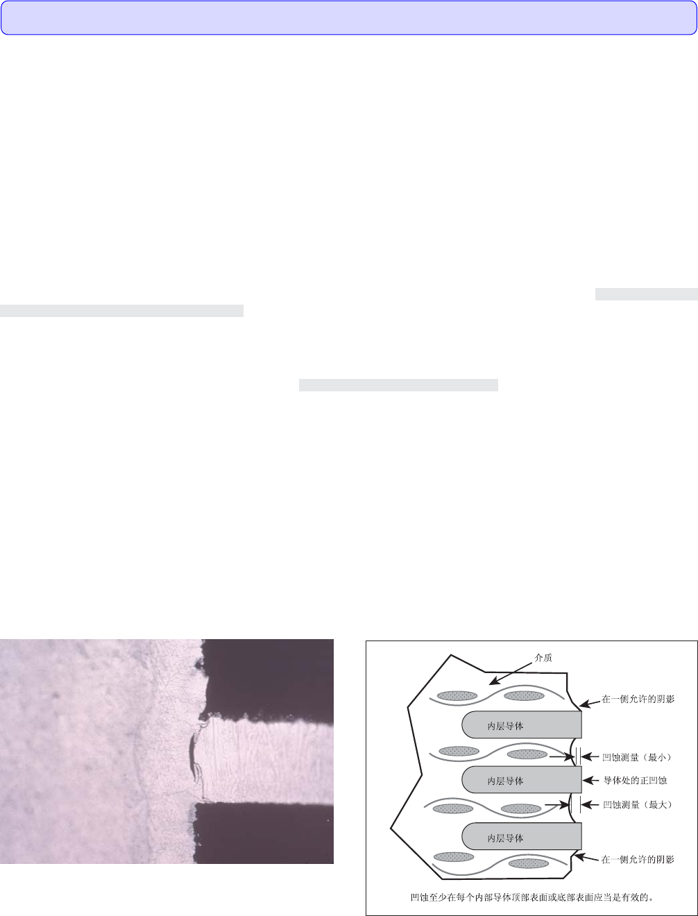
Acceptable etchback or negative etchback exhibits the evidence that resin smear has been removed from the innerlayer copper/ drilled hole
interface. An example of resin smear appears in Figure 315a. There is data, pro and against, that etchback is more reliable than negative etch-
back and vice versa. This all depends on what type of copper plating, copper foil, and weight of the foil being used. Excessive etchback as
well as excessive negative etchback are not the target condition. Excessive etchback, in both instances, has an adverse effect on the reliabil-
ity of the PTH life.
可接受的凹蚀或负凹蚀表现为树脂钻污已经从内层铜箔与钻孔界面处清除干净。图315a为钻污的一个例子。有数据表明,“凹
蚀”要比“负凹蚀”更为可靠,但也有相反的观点,这取决于所采用的电镀铜、铜箔的类型及铜箔的厚度。过度的凹蚀以及过度
的负凹蚀都不是理想状况。这两种情况下的过度凹蚀对镀覆孔的可靠性都会造成负面影响。
Etchback: The etchback process, also known as positive etchback, is used to remove the dielectric material. The evidence of resin mate-
rial being etched back theorizes that all resin smear has been removed and in addition, a three way interfacial bond occurs between the PTH
copper to the innerlayer copper foil. The theory is that three connections are more reliable than one. The drawbacks of etchback are that it
creates rough holes which could create PTH barrel cracks. Excessive etchback also contributes to stresses that might create foil cracks. Shad-
owing is defined as a condition that occurs during an etchback process in which the dielectric material immediately next to the foil is not
removed completely. This can occur even though an acceptable amount of etchback may have been achieved elsewhere. Proper measurement
locations for etchback are shown in Figure 315b.
凹蚀:凹蚀过程,也称之为正凹蚀,用于去掉介质材料。树脂材料被凹蚀的迹象说明,所有的树脂钻污已被完全去除,同时镀覆
孔的铜和内层铜箔之间产生出三维界面的结合。三维连接比一个界面连接更加可靠。但缺点是凹蚀会造成孔壁粗糙,使孔壁产生
裂缝。过度的凹蚀也会导致可能引起内层铜箔破裂的应力。凹蚀阴影是指在凹蚀过程中,紧靠铜箔的树脂并未被完全清除。这种
情况即使在别处已达到可接受的凹蚀情况时也会发生。适当的凹蚀测量位置如图315b所示。
Negative Etchback: The theory here is that in order for the internal foil to be etched back/cleaned, you need to eliminate the smear. The
benefits for utilizing negative etchback are that the process does not create a stress point at the internal plane, as does the etchback process,
and it results in a very smooth/uniform copper barrel hole wall. The smooth hole wall and negative etchback are beneficial especially for the
copper plating of high-reliability long term life applications. The drawback of negative etchback, if excessive, is that it may create innerlayer
separation due to entrapped air pockets/contamination. This section is not intended to prove or disprove which etchback process is preferred.
There are many printed board manufacturers that are very successful in utilizing both the etchback and negative etchback processes. It is up
to the individual designer/user, depending on the material, copper plating, copper foil and application, to specify which etchback process
should be employed.
负凹蚀:其理论是:为了将内层铜箔凹蚀又清洁,首先要把钻污全部清除。负凹蚀的优点是不会像凹蚀那样在内层界面处产生应
力集中点,负凹蚀可以形成一个非常平滑而均匀的孔壁。平滑的孔壁及负凹蚀对于高可靠、长寿命应用的铜镀层特别有利。负凹
蚀的缺点是,如果负凹蚀过度,由于凹处夹留气泡和污染物,可能引起内层分离。本节无意于对优先选用哪种凹蚀工艺表示赞成
或反对。有很多印制板制造商不管是采用凹蚀还是负凹蚀工艺都很成功。应该采用哪种特定的凹蚀工艺,取决于各个设计者或用
户,同时也取决于所采用的材料、铜电镀、铜箔和应用等因素。
图315a 去钻污实例
图315b 凹蚀测量
3.1 DIELECTRIC MATERIALS(介质材料)
3.1.5 Etchback(凹蚀)
81IPC-A-600H-2010 2010年4月
Visual observations made on cross-sections only.(仅对显微切片进行目检观察。)