IPC-A-600H-2010 中文版 印制板的可接受性 (1).pdf - 第27页
造 成白斑 /微 裂 纹 状况的因 素 还 有: 树脂 的 成 分、 层 压 方法、 耦 合 剂 , T g 等。 过 去搜集 到的 报告 显示, 白斑 和微 裂 纹 范 围超 过 间距 的 50% 以上时, 也 不 会 影响 硬 件的可靠性。 既 然 所有 测试 报告 都 显示 白斑 没有问题, 而且 没有使用 失 效的 报告 , 为 什么我们 还 如此 顾虑 白斑 和微 裂 纹 现象 呢? 因为理 论 上 看 来 ,如 果导 体之 …

Even when the potential failure mechanism mentioned above is
analyzed, it is almost impossible to experience such (IR/ migration)
failure. First, a measle(s) gapping conductive patterns is needed.
Secondly, moisture in the printed board/ assembly, along with a
conductive or ionic contaminant such as chlorides, is necessary.
In this instance, a typical industry example, the measle is at the
center between two plated through holes (see Figure 23b). The
measle is 0.4 mm [0.0157 in] wide. In order to get possible copper
migration, the measle had to gap the two plated through holes. This
of course would be most unlikely. The second example (see Figure
23c) illustrates what is required for a potential failure mechanism
between two surface conductors. A (+) conductor directly over a
knuckle is required and a (-) conductor is also required directly over
a knuckle. For an electrical short to occur between these conductors
through the base material, there would need to be a conductive path
from one conductive pattern, through the remaining dielectric
materials (resin and yarn) to the separation (measle), along the
separation in the direction of the other conductive pattern, once
again through the remaining dielectric materials (resin and yarn),
and to the second conductive pattern. In order to induce a failure all
of the above mentioned ingredients are required along with a volt-
age potential between two adjacent conductors. This occurrence is
highly unlikely and is most likely why the industry has not experi-
enced any adverse reliability problems due to measles.
When making acceptance calls on electronic hardware, consider all
the possible concerns mentioned above. Measles should not be con-
sidered a nonconforming condition. It should instead be considered
a process indicator, telling you that the process is on the verge of
going out of control. Correct the problem, but do not scrap the
product, taking into account all of the above mentioned variables.
第⼆届IPC蓝带委员会关于⽩斑的概述
第二届委员会成立于1978年底。它复审了第一届委员会的发
现,向业界征寻了更多的数据资料,并审阅了IPC会员提供的
专有验收准则。第二届蓝带委员会得出了同样的结论。白斑
是一种外观性的制程警示,在大多数应用中,几乎没有任何
有关影响产品性能的报道。一个主要的例外是高压电应用。
此时仍有一些政府机构和业界公司反对无条件地接受白斑。
因此,该委员会制定了一套由所有IPC会员一致同意的白斑/
微裂纹要求。形成的验收要求适用于印制板电子组装过程中
三个主要阶段:层压板材料、印制板终检和印制板组装后。
这些要求包括导体间距减小的百分比(不超出最小的导体间
距)和基于产品级别的印制板(或组装件)每面的白斑区域
的大小。这些要求作为修订本补充到IPC-A-600C版的首印版
中,并纳入IPC-A-600C的再版中,且在IPC-A-600D版中以不
同形式出现。
说明:反对方阐明的主要顾虑归纳如下:
• 电气绝缘电阻,包括体积电阻和表面电阻 - 一些报告和现
有的测试数据都表明:绝缘电阻受白斑或微裂纹的影响不明
显。
• 污染 - 离子残留物可能会扩散或被“抽吸”(由于大气压发
生变化)到白斑或微裂纹中,并会导致绝缘电阻的降低或导
电阳极丝(CAF)的生长进而短路。盐雾测试表明,这个根
据不能成立,大多数离子物(例如盐)不会扩散到基材中。
• 所用电压 -高压应用关系是一个顾虑(尤其是白斑或微裂
纹中可能出现“电晕”的情况下),与类似的无白斑/微裂纹
区域相 比,有白斑/微裂纹的区域的绝缘强度降低了20%~
50%,尤其在20km(12.43英里)以上的海拔高度下。
• 环境
- 大
多数白斑/微裂纹不会因环境测试而增加或尺寸扩
大。
IPC-A-600E版本是第一个反映表面贴装元器件技术需求的修
订版。因此,对白斑和微裂纹的验收要求便分开了。就白斑
而言,验收要求允许其跨接表面导体间距。这样规定基于白
斑的定义、测试数据,而且业界的经验中从来没有白斑导致
功能性失效的记载。微裂纹是产生于基材内的一种更不受控
的分离现象,形成白斑间的互连,其范围可能跨接相邻的导
电图形,因此,对白斑的验收要求与类似的分层和起泡状况
相同。
相当长一段时期,一些指导规范过于看重白斑现象。再者,外
观也成为一个主要的验收准则。事实上,迄今为止,根据所
有军方及工业界当前测试发现,白斑从未导致过任何失效。
IPC、业界及各军方机构在极端环境条件下,对出现严重白斑
的组件进行了广泛的测试,并没有发现白斑有增长、扩散或
有损于组件功能的现象。白斑不应该作为拒收的理由。
白斑是发生在编织纤维增强型层压基板内的一种内在现象,
基材内的纤维纱束在交叉处的粘合发生分离。“微裂纹”一
词有时用来描述表面上连成片的白斑阵列现象。这种称作微
裂纹的互连的白斑,其实是分层的一种形式,即纤维纱线沿
其长度方向与树脂发生了分离。对于非编织的材料,这种情
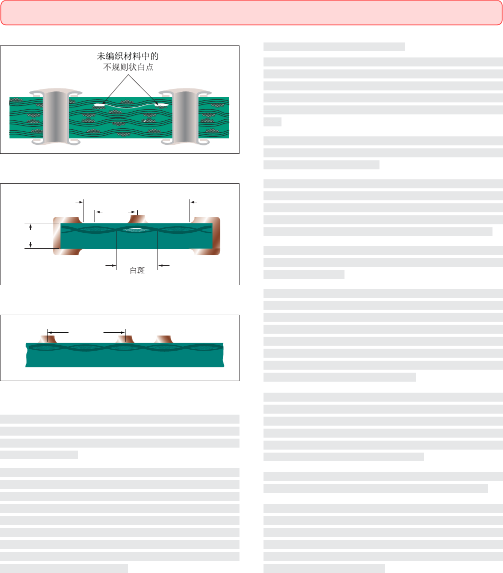
况类似于白斑但是随意排列且形状不规则(见图23a)。
在一项研究案例中,所观察到的白斑现象主要成因是能快速
扩散到环氧玻璃中的湿气和元器件焊接时的温度共同作用的
结果。元器件贴装时产生的局部高温造成裹挟的湿气蒸发,
并破坏环氧玻璃在“接合点”(环氧玻璃布经线与纬线交叉
处)的粘合。根据以往的经验,我们知道环氧玻璃会吸收大
气中的湿气,当湿气含量超过0.3%(重量比)时,在浸焊/热
风整平和/或组装焊接作业中会使白斑增加。
2.3
BASE
MATERIAL SUBSURFACE(基材表⾯下)
Introduction (cont.)(引⾔(续))
18 IPC-A-600H-20102010年4月

造成白斑/微裂纹状况的因素还有:树脂的成分、层压方法、
耦合剂,T
g
等。过去搜集到的报告显示,白斑和微裂纹范围超
过间距的50%以上时,也不会影响硬件的可靠性。既然所有
测试报告都显示白斑没有问题,而且没有使用失效的报告,
为什么我们还如此顾虑白斑和微裂纹现象呢?因为理论上看
来,如果导体之间布满白斑,同时伴有湿气或其他污染物,
那么在导体之间应该存在铜的迁移(即绝缘电阻失效)。
尽管上文分析了潜在的失效机理,但出现这样的失效(绝缘
电阻或迁移)几乎是不可能的。首先需要白斑填满导电图形
之间。其次,印制板/组件内需要有潮气,并伴有导电的或离
子的污染物,例如氯化物。
图23b图示了业界的一个典型实例,白斑位于两个镀通孔间的
中心处(见图23b),其宽度为0.4mm[0.0157in]。要想使铜迁
移成为可能,白斑必须占满两个镀覆孔之间的区域。这种情
况当然是不太可能发生的。另一个案例(见图23c)图示了两
个表面导体之间存在潜在失效机理的条件。它要求一根带正
(+)电的导体刚好落在纤维交织点上,同时还要求另一个带
负(-)电的导体也刚好落在纤维交织点上。要想这两个导体
通过基材产生电气短路,需存在以下这样一条导电通路:从
一个导电图形开始,经由尚存的介质材料(树脂和纤维)到分
离点(白斑),沿着分离处向另一个导电图形的方向,再经过
尚存的介质材料(树脂和纤维),最后到达另一个导电图形。
上述条件均符合的情况下,还需要这两个相邻导体之间有压
差。这是非常不可能的事情。这也是为什么业界至今尚无任
何由于白斑造成可靠性问题的原因。
确定电子组件验收准则时,要考虑上述所有可能发生的情
况。不应该把白斑看作不符合条件。应该将白斑看作为制程
警示,它告诉你制程正面临失控的可能。纠正问题,而不是
报废产品,分析上述种种可能,排查隐患。
Brief summary of the Third IPC Blue Ribbon Committee on
Measles
In 2004, the issue of printed board laminate degradation caused by
internal Conductive Anodic Filament (CAF) growth came to the
forefront of discussions among the IPC printed board assembly
standards groups (including the 7-31b IPC-A-610 and 5-22a
National Standard for Soldering task groups.) It was observed that
circuit density, operating speed, band pass and reduced operating
voltage had impacted the ability of circuits to operate under condi-
tions supporting dendrite or CAF development.
With the proliferation of finer line conductors and reduced spacing
in current designs, discussions within the assembly standards
groups questioned the role of measles within printed board lami-
nate materials as a potential catalyst for CAF growth.
For years, IPC standards for electronic production contained no
restrictions for the occurrence of measles in printed boards and/or
assemblies. Theoretically, measles could be continuous between
conductors and could exist throughout the printed board. It was
noted that this allowance was based on studies conducted nearly 30
years earlier based on circuit designs from that time period. It was
recognized that a need existed to reconsider the measles require-
ments for today's production designs and product environment.
In the interim, as a means to call attention to this potential problem,
IPC assembly documents were changed to include pass/fail (defect)
criteria for Class 3 assemblies that exhibited the visual appearance
of measles.
The new measles criteria created in the assembly documents
defined requirements that were stricter than those given in the
printed board documents unless the additional IPC-6012, Class 3A
(Military and Aerospace) requirements were considered. IPC-
6012, Class 3A does not allow measles in bare boards for these
industry segments, however Class 3 printed boards produced in
accordance with 6012, which exhibited measles, were no longer
acceptable for use in the assembly documents for Class 3 in gen-
eral. This requirement conflict was brought to the attention of the
IPC Technical Activities Executive Committee (TAEC) and that
body directed both groups to work together to come to some reso-
lution, based on test data that would bring the documents into
agreement on the acceptance criteria.
The leadership of the printed board standards committees formed a
new Blue Ribbon Committee on Measles and designed and per-
formed testing to determine if measles contributed to CAF failures
in actual end product. This test protocol was completed in late 2006
and presented to the printed board standards committees at IPC
Printed Circuits Expo/APEX 2007. There was conclusive evidence
within the test that measles did not contribute to CAF growth; nor
did the presence of measles promote CAF failures in the end prod-
uct that exhibited CAF.
2.3 BASE MATERIAL SUBSURFACE(基材表⾯下)
Introduction (cont.)(引⾔(续))
19IPC-A-600H-2010 2010年4月
This presentation was then given to the assembly standards groups
for their consideration. The request was made that the requirements
in the bare printed board and assembly documents be changed to
track with each other.
The leadership of the assembly standards groups concurred that the
industry now had test data that addressed their original concerns
regarding the potential of measles to promote CAF failures. They
also agreed that the documents should be amended to eliminate the
conflicting measles requirements. The groups jointly drafted the
words, comments, and instructions for all documents regarding
measles and these were presented to the committee membership at
the 2007 IPC Midwest Conference. Copies of the test protocol sum-
mary are available through the IPC.
第三届IPC蓝带委员会关于⽩斑的概述
2004年,由于内部导电阳极丝(CAF)生长造成的印制板基
材质量退化问题在IPC印制板组装标准工作组(包括7-31b
IPC-A-610和5-22a国家焊接标准任务工作组)中成为了讨论
的焦点。据观察,电路密度、运行速度、通带、工作电压的
降低在有利于结晶或CAF生长的条件下均对电路的运行有影
响。
随着电流设计中细线条导体的增加和导体间距的减少,组装
标准工作组 对印制板基材中白斑的作用提出了疑问,认为
其是CAF生长的潜在催化剂。
多年来,IPC电子生产的标准中均未涵盖对印制板和/或组装
板中白斑现象的限制。从理论上讲,白斑可能在导体之间连
续呈现,也可能存在于整块印制板。大家注意到了这种允许
规定是基于30年前在当时电路设计上的研究。大家认识到有
需要针对当今的生产设计和产品环境重新考虑白斑的要求.
在此期间,为了引起对这一潜在问题的关注,IPC对组装文件
作了变更,变更涵盖了对3级组装件中白斑外观的合格/不合
格(缺陷)的准则。
除了考虑采用IPC-6012中3A级(军用和航空)要求,否则在
组装文件中建立的关于白斑的新准则比印制板文件中规定的
要求更严格。IPC-6012中3A级不允许在这些行业领域的裸板
上出现白斑,但是,按照6012生产的3级印制板出现白斑时,
如用于组装3级产品,通常是不可接受的。这一要求的矛盾引
起了IPC技术活动执行委员会(TAEC)的关注,在该委员会
的指导下,两个工作组一起努力找到了解决方案,根据测试
数据,使文件中的验收准则达到一致。
在印制板标准委 员 会 的 领导下,成立了新的白斑蓝带委员
会。该委员会设计并进行了实验以确定白斑是否是实际整机产
品中CAF失 效的原因。该实验程序于2006年后期完成,并于
IPC
2007
印制板展览会/APEX期间提交给印制板委员会。其
测试的总结性证据说明白斑不是CAF生长的起因,也不是出现
CAF的整机产品中CAF失效的促成原因。
该报告后期已提交给组装标准工作组,提请他们考虑更改组
装文件,以使裸印制板文件和组装文件的要求互相一致。
组装标准工作组的领导一致同意,提出现在行业中已有测试
数据解决了他们对潜在白斑引发CAF失效的最初顾虑。委员
会同时 同 意对文件进行修订从而排除对白斑要求的矛盾之
处。工作组联合起草了所有文件中关于白斑的文字、意见和
建议,并于2007年IPC中西部会议期间提交给委员会成员。该
测试程序总结可通过IPC获得。
图23b ⽩斑跨接了导电图形的案例
注:此图仅⽤作说明状况,并不要求做显微剖切评价。
0.35 mm
[0.0138 in]
0.25 mm
[0.00984 in]
0.40 mm
[0.0157 in]
1.00 mm
[0.040 in]
图23c 两个表⾯导体之间潜在失效机理的案例
注:此图仅⽤作说明状况,并不要求做显微剖切评价。
0.80 mm
[0.031 in]
+-+
图23a 微裂纹案例
注:此图仅⽤作说明状况,并不要求做显微剖切评价。
2.3 BASE MATERIAL SUBSURFACE(基材表⾯下)
Introduction (cont.)(引⾔(续))
20 IPC-A-600H-20102010年4月