YSi-SP_Ope_E.pdf - 第107页
2-70 2 Operation 4.2.1 Image Editing Edit inspection pads, zero level and fiducial marks. 1. T ouch the [edit] button to open the screen shown below . 3 2 242A0-KMN-00 2. Select the editing item among the [Insp pad], [Ze…
2-69
2
Operation
4.2 Editing PCB Data
Edit the created inspection program.
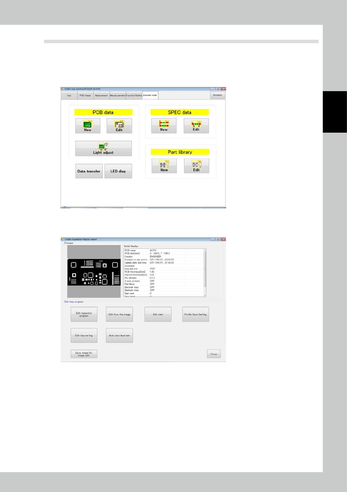
To edit the inspection program, you must log in at the engineer privilege.
Touch the engineer mode tab on the main menu to open the engineer mode screen.
Select [Edit] or [Light Adjust] for the PCB data to edit the program.
24298-KMN-00
1. To edit data other than the light intensity, touch the [Edit] button.
2. Select details of editing according to the editing wizard.
24299-KMN-00
2-70
2
Operation
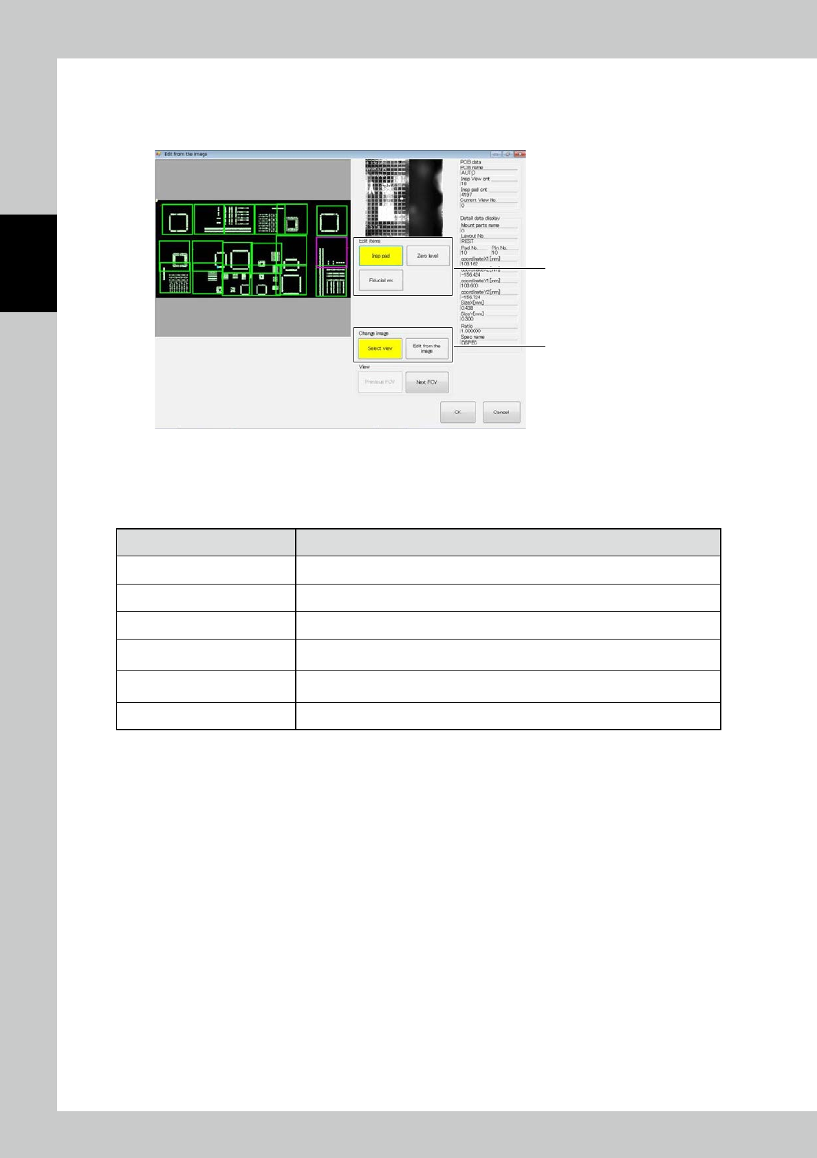
4.2.1 Image Editing
Edit inspection pads, zero level and fiducial marks.
1. Touch the [edit] button to open the screen shown below.
3
2
242A0-KMN-00
2. Select the editing item among the [Insp pad], [Zero level] and [Fiducial mk] buttons.
3. Select the desired editing operation. The displayed options vary according to the button selected in step 2.
■
Description of screen
Name Function
Image The image of the whole PCB and the image of the selected field of view are displayed.
PCB data The data about the selected PCB is displayed.
Detail data The detail data about the selected pad is displayed.
[Select view] button
The image of the whole PCB is displayed on the left side in a large size. This function is
useful to view the entire PCB or select the field of view.
[Edit from the image] button
The image of the field of view is displayed on the left side in a large size. This function
is useful to finely adjust the pad or zero level.
[Previous FOV] / [Next FOV] button Move the selected field of view to a previous or next one.
2-71
2
Operation
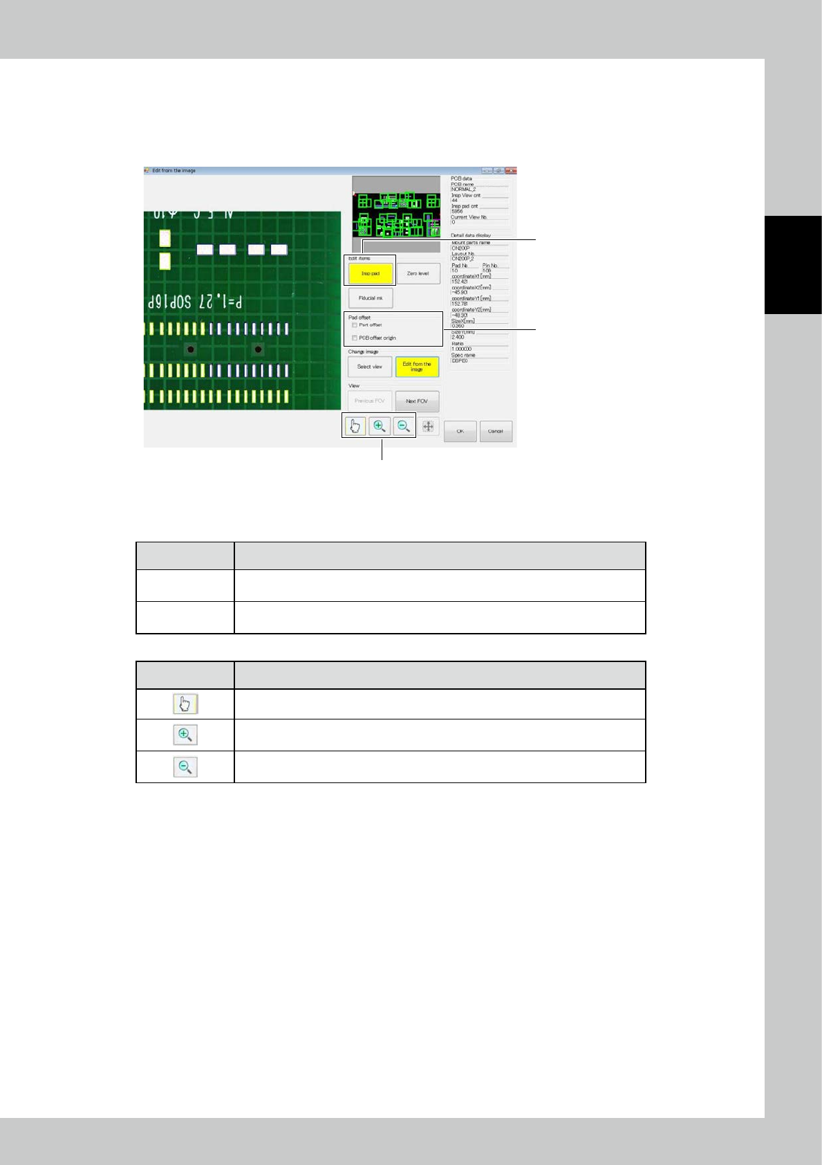
1. Inspection pad
The position or size of the inspection pad is changed, copied or deleted.
Pad offset function
With this function, the inspection pad moves by an offset. Drag and drop the desired pad to move the pad by an offset.
2
3
1
242A1-KMN-00
1. On the screen shown above, select the [Insp pad] button.
2. Place a check mark to simultaneously move multiple pads by an offset.
Name Function
Parts offset
You can change the position of inspection pads of a part. Drag and drop one of
inspection pads to change the position of pads having the same layout number.
PCB offset origin
The entire PCB moves by an offset. Drag and drop a single pad in the PCB to
move all pads simultaneously.
3. Touch the desired pad to be moved by an offset, and drag and drop it. The pad moves.
Name Function
In case of the zoom-in or -out mode, the edit mode starts.
Start the zoom-in mode. If the field of view image is clicked on in the zoom-in mode,
the image is enlarged around the designated point.
Start the zoom-out mode. If the field of view image is clicked on in the zoom-out
mode, the image is reduced around the designated point.