YSi-SP_Ope_E.pdf - 第99页
2-62 2 Operation 1 2 5 3 4 24286-KMN-00 Adjust the light intensity for solder e xtraction and click on the [>>] button. ■ Description of screen No Name Description of displayed item and functions 1 Buttons Use butt…
2-61
2
Operation
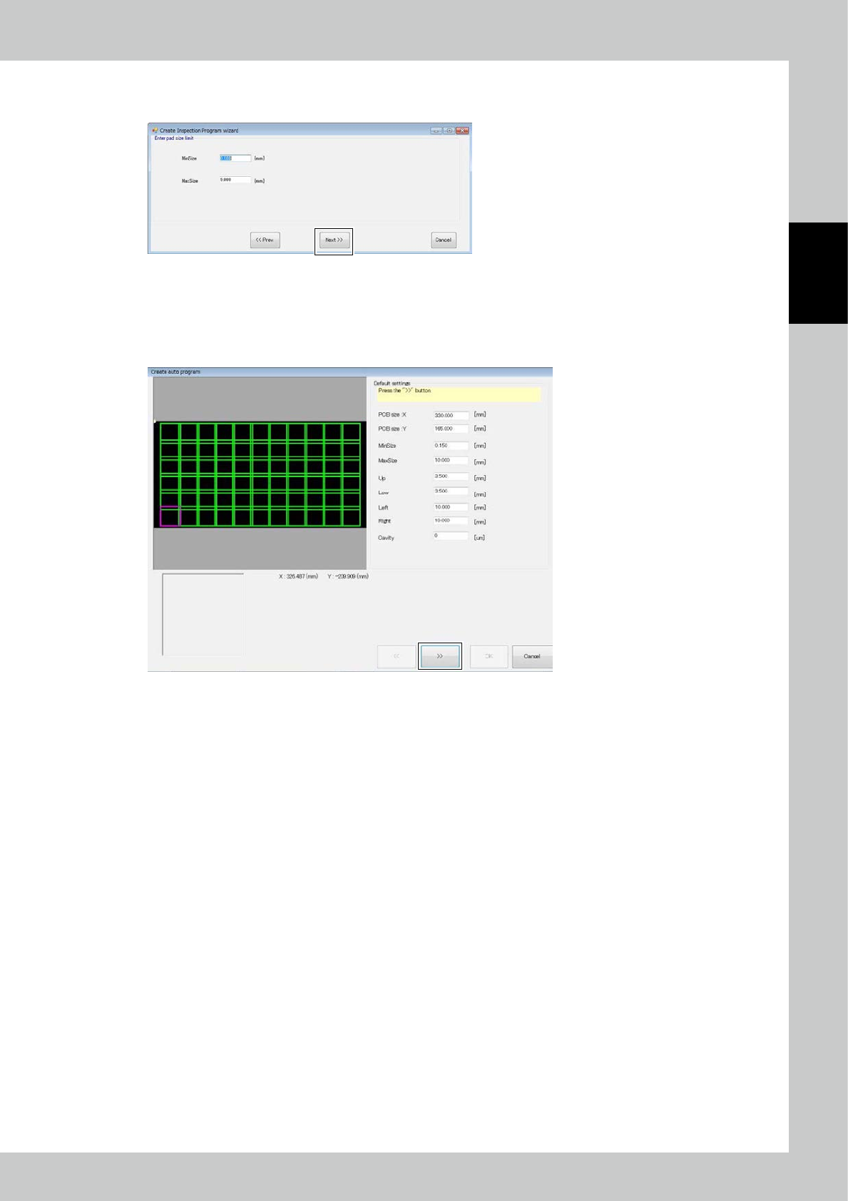
Enter the pad recognition range values.
Click on the [Next] button.
24284-KMN-00
The image of the PCB is displayed. The image shows the pad extraction range and the number of fields of view, based on
the entered PCB data.
The entered values are displayed on the right side of the screen. You can modify values to adjust the PCB image.
After confirmation or adjustment is finished, click on the [>>] button.
24285-KMN-00
2-62
2
Operation
1
2
5
3
4
24286-KMN-00
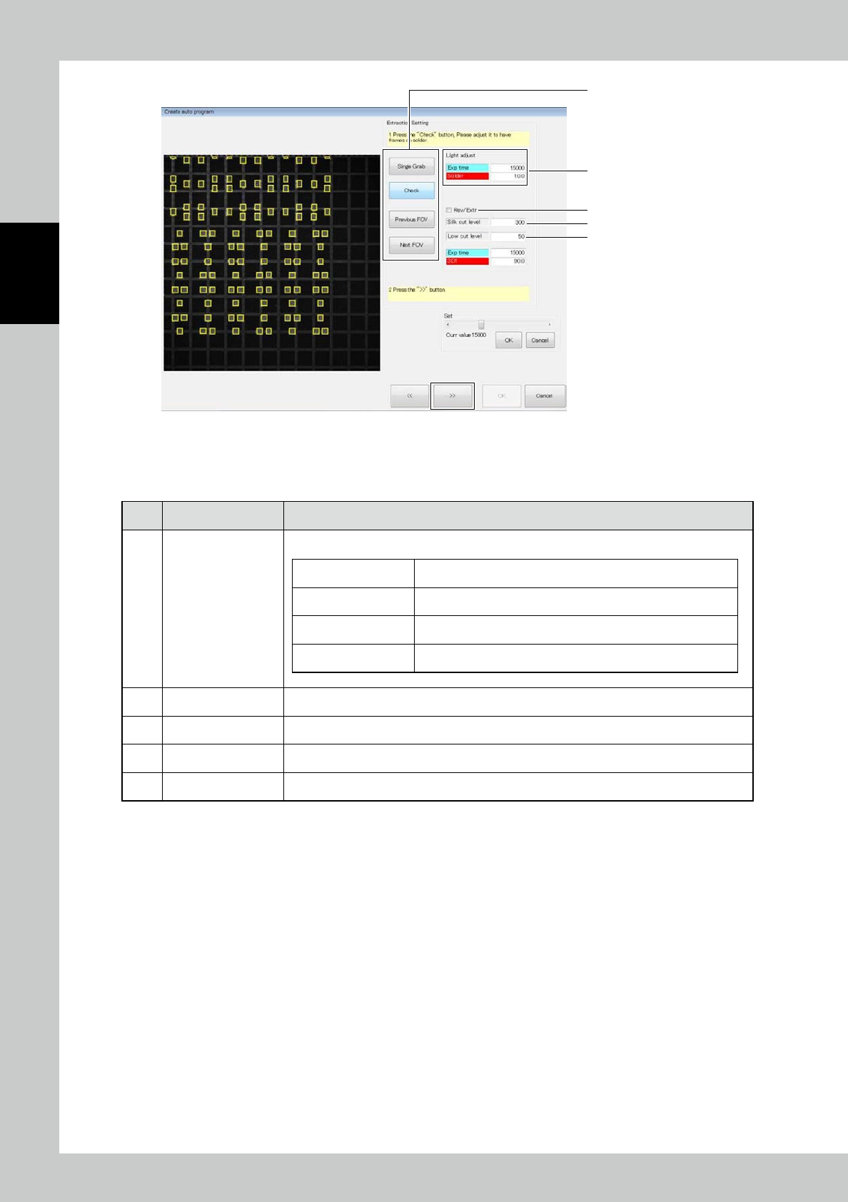
Adjust the light intensity for solder extraction and click on the [>>] button.
■
Description of screen
No Name Description of displayed item and functions
1 Buttons
Use buttons to adjust the light intensity.
[Single Grab] button The selected field of view is acquired once.
[Check] button An extraction test of the selected field of view is performed.
[Previous FOV] button The field of view changes to the previous one.
[Next FOV] button The field of view changes to the next one.
2 Adjust light intensity Adjust the number in the table to adjust the light intensity.
3 Silk level Adjust the level of the silk cut.
4 Height cut level Adjust the height cut level.
5 Rev/Extr The extracted image is reversed for extraction.
2-63
2
Operation
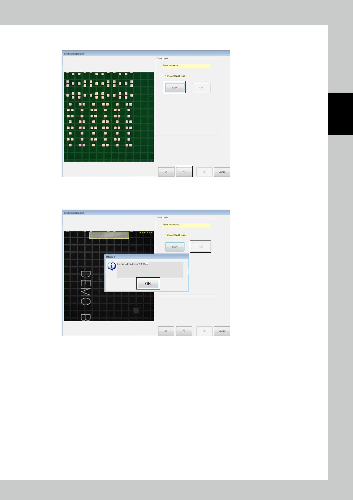
Click on the [Start] button to start to extract pads.
After pad extraction is finished, click on the [>>] button.
24287-KMN-00
To interrupt pad extraction in the middle, click on the [Abrt] button.
The above window opens with the number of extracted pads. Click on the [OK] button.
24288-KMN-00