YSi-SP_Ope_E.pdf - 第119页
2-82 2 Operation 8. Bad Mark 4 1 3 5 2 242B5-KMN-00 1. T ouch the [Bad mark] tab. TIP The bad mark tab is displayed only if a bad mark is registered in the inspection program. 2. Select the light sour ce to be used and a…
2-81
2
Operation
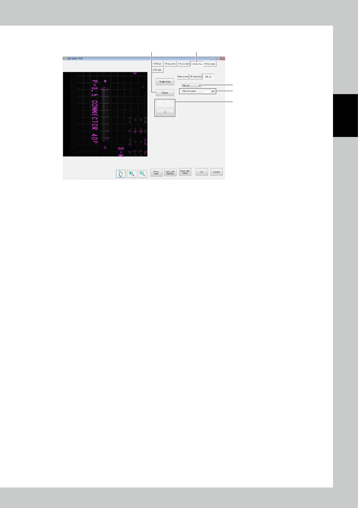
7. Silk cut
3
5
1
2
4
242B4-KMN-00
1. Touch the [Solder Insp] button. Touch the [Silk Cut] button.
2. Touch the [<<] or [>>] button to select the field of view.
3. Touch the [Check] button to display the result on the screen.
Check whether the silk part of the PCB and the exposure part of the electrode turn to pink color.
The pink colored part is the part which shall be silk-cut.
4. Adjust the [Silk Cut Level] so that the silk part becomes pink.
5. To invalidate silk cutting, select [No insp].
2-82
2
Operation
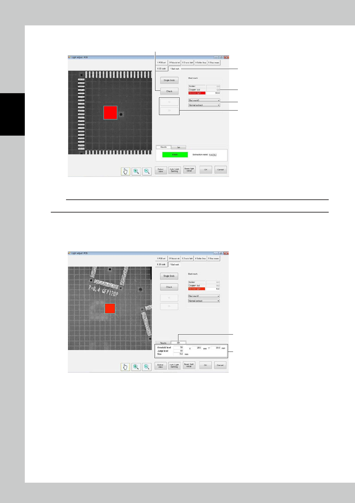
8. Bad Mark
4
1
3
5
2
242B5-KMN-00
1. Touch the [Bad mark] tab.
TIP
The bad mark tab is displayed only if a bad mark is registered in the inspection program.
2. Select the light source to be used and adjust the light intensity.
3. When necessary, select Normal extract or Rev/Extr.
4. Touch [<<] or [>>] to select the bad mark to be checked.
5. Touch
[
Check] to show results.
6
7
242B6-KMN-00
6. To adjust the bad mark position or the like, touch the Set tab.
7. Adjust the
[
threshold level], [Judge level], [Size] and coordinates so that the bad mark is extracted correctly.
2-83
2
Operation
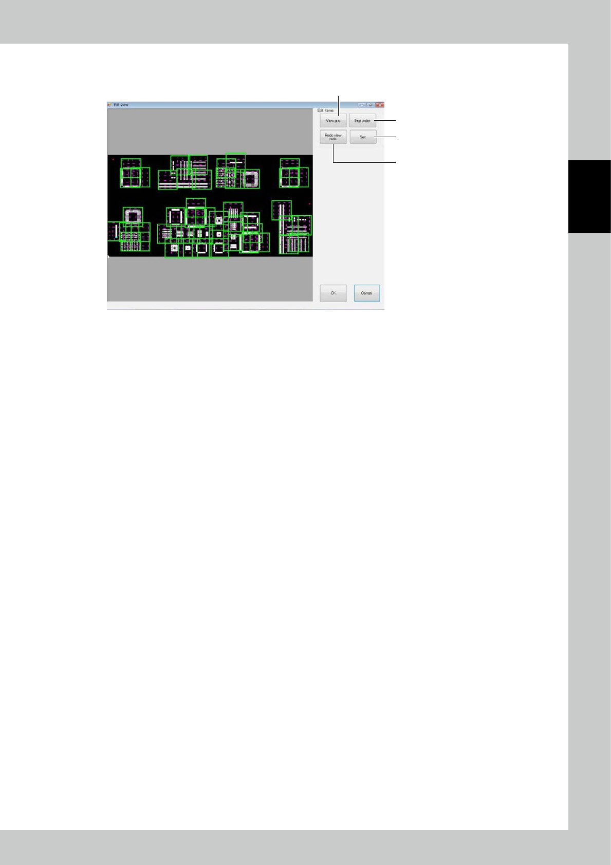
4.2.4 Field of View Editing
1
2
4
3
242B7-KMN-00
1. [View pos] button
Change the field of view position. If a zero level moves out of the field of view when the field of view position is
changed, a confirmation message is displayed.
2. [Insp order] button
The inspection order (moving path of the camera of the inspection machine) of the field of view is changed.
3. [Redo view ratio] button
All fields of view are automatically divided again.
4. [Set] button
The effective range of the field of view is changed.