YSi-SP_Ope_E.pdf - 第64页
2-27 2 Operation T he solder style can be switched in the follo wing wa y . 1. Cross Selection 2. Solder image 3. Cut level PCB data: The PCB data is displayed. Inspection result: The inspection results of the selected p…
2-26
2
Operation
3.4.1 Profile Screen
The items displayed in the profile screen and functions are described.
6 9 87 10 11
4
12
3
5
1
2
24226-KMN-00
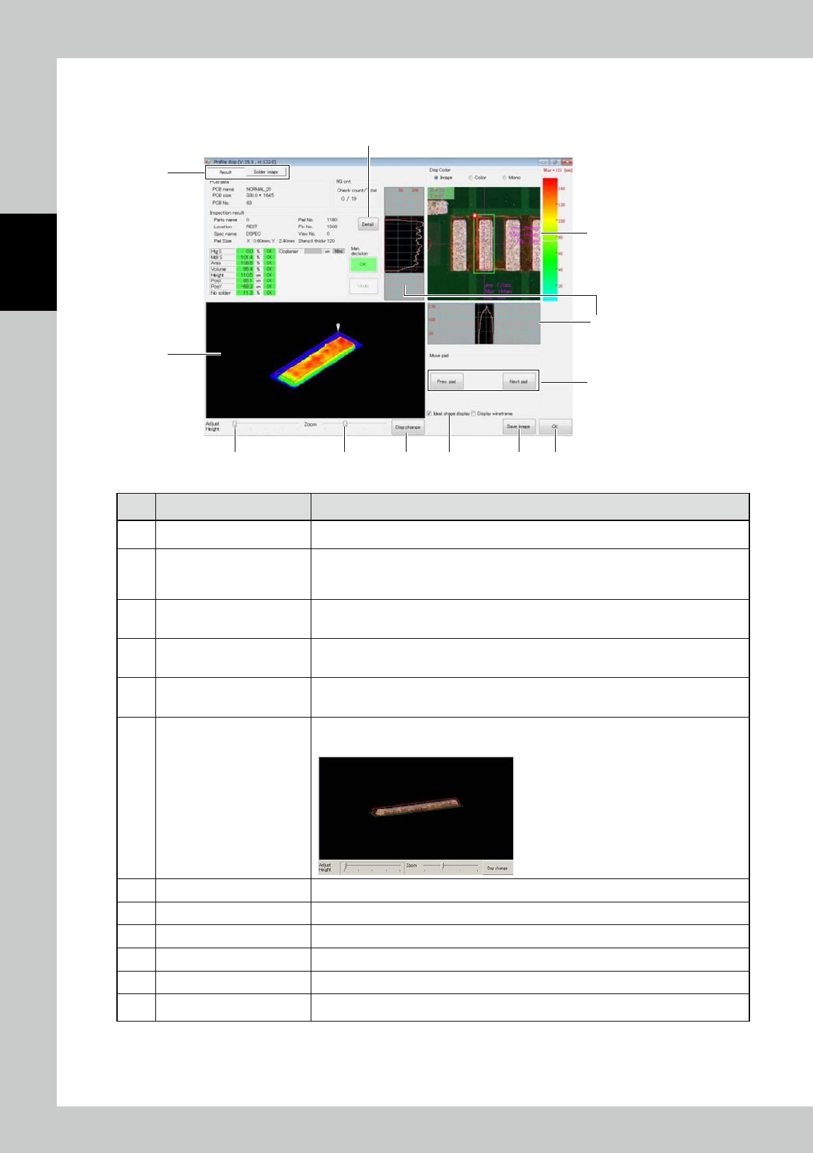
No Name Description of displayed item and functions
1 Display selection
Select the profile displaying style. Use the corresponding tab to select pad inspection
result, solder image or horizontal cross section.
2 3D image
The 3D image of the designated pad is displayed. The red wire frame around the pad
indicates the ideal profile based on the area of the opening of the metal mask and mask
thickness, indicating the approximate volume fill ratio. Move a finger along the 3D image to
change the displaying angle vertically or horizontally over 360° as you need.
3 2D image
This is the top view image of the pad with colored height discrimination. For the relationship
between the height and color, see the following description.
The displayed image can be selected among "Image," "Color," and "Mono."
4 Cross section graph
This is the cross section shape of the pad located at the cross on the 2D image (3). Touch
an arbitrary part of the 2D image to change the cross location. The data displayed outside
the image indicates the maximum value, minimum value and average.
5 [Prev pad] / [Next pad] button
The pad, the profile of which is displayed, is changed in the order of the pad number.
In the faulty or warning pad display mode, the previous or next faulty or warning pad is
displayed.
6 Adjust dsp height
Move the slide to adjust the solder height of the 3D image.
The height profile of the solder is intensified in the displayed image.
7 Zoom Adjust the displaying scale.
8 Ideal shape display Place a check mark to display a wire frame of the ideal shape of the solder. (See above 2).)
9 [Dsp change] button The color gradation height indication is reflected on the 3D image.
10 [Save image] button The current images are saved in the PC of the inspection machine.
11 [OK] button Exit to return to the measurement screen.
12 [Detail] button The judgment results of pad inspection are displayed.
2-27
2
Operation
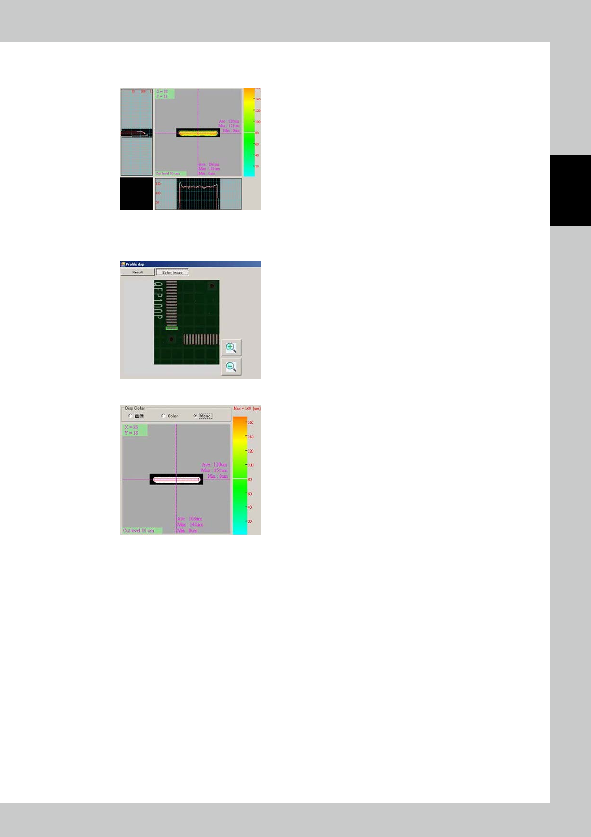
The solder style can be switched in the following way.
1. Cross Selection
2. Solder image
3. Cut level
PCB data: The PCB data is displayed.
Inspection result: The inspection results of the selected pad are displayed.
24228-KMN-00
The cut level image is displayed in colors corresponding to the color gradation graph.
Touch the graph to determine the height of the cross section.
Color gradation graph: [High] red <=> orange <=> yellow <=> green <=> blue [Low]
2-28
2
Operation
3.4.2 Wide Area Measurement Screen
Items displayed on the wide area measurement screen and functions are described.
7 5
8
9
6
4 10
3
2
1
24229-KMN-00
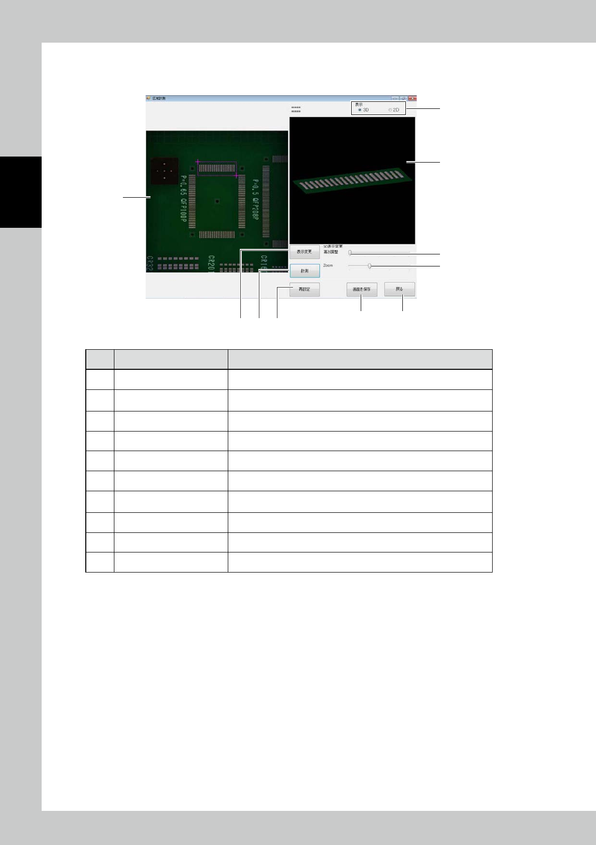
No Name Description of displayed item and functions
1 Image of field of view The image of the currently selected field of view is displayed.
2 3D image
The 3D image of the area designated as a measurement range on the field
of view screen is displayed.
3 Disp Disp 3D/2D
4 [Save screen] button Save the currently displayed screen.
5 [Reset] button The current selected area is canceled.
6 [Measurement] button The range selected in the view image is displayed in a 3D image.
7 [Dsp change] button
The 3D image changes to a normal image or color gradation height
discrimination image. The view alternates each time the button is touched.
8 Adjust disp height Change the scale of the displaying height.
9 Zoom in / Zoom out Change the scale of the displayed image.
10 [Return] button Return to the measurement screen.