YSi-SP_Ope_E.pdf - 第97页
2-60 2 Operation Enter dimension of PCB and thickness of metal mask. Repeat the step to choose a width setting if required. Convey PCBs to take them in the mac hine. Click the [Next] button. 24281-KMN-00 Enter the coordi…
2-59
2
Operation
4. Inspection Program
4.1 Creating new PCB data (printed PCB)
The method for creating an inspection program using the taken image of a printed PCB is described.
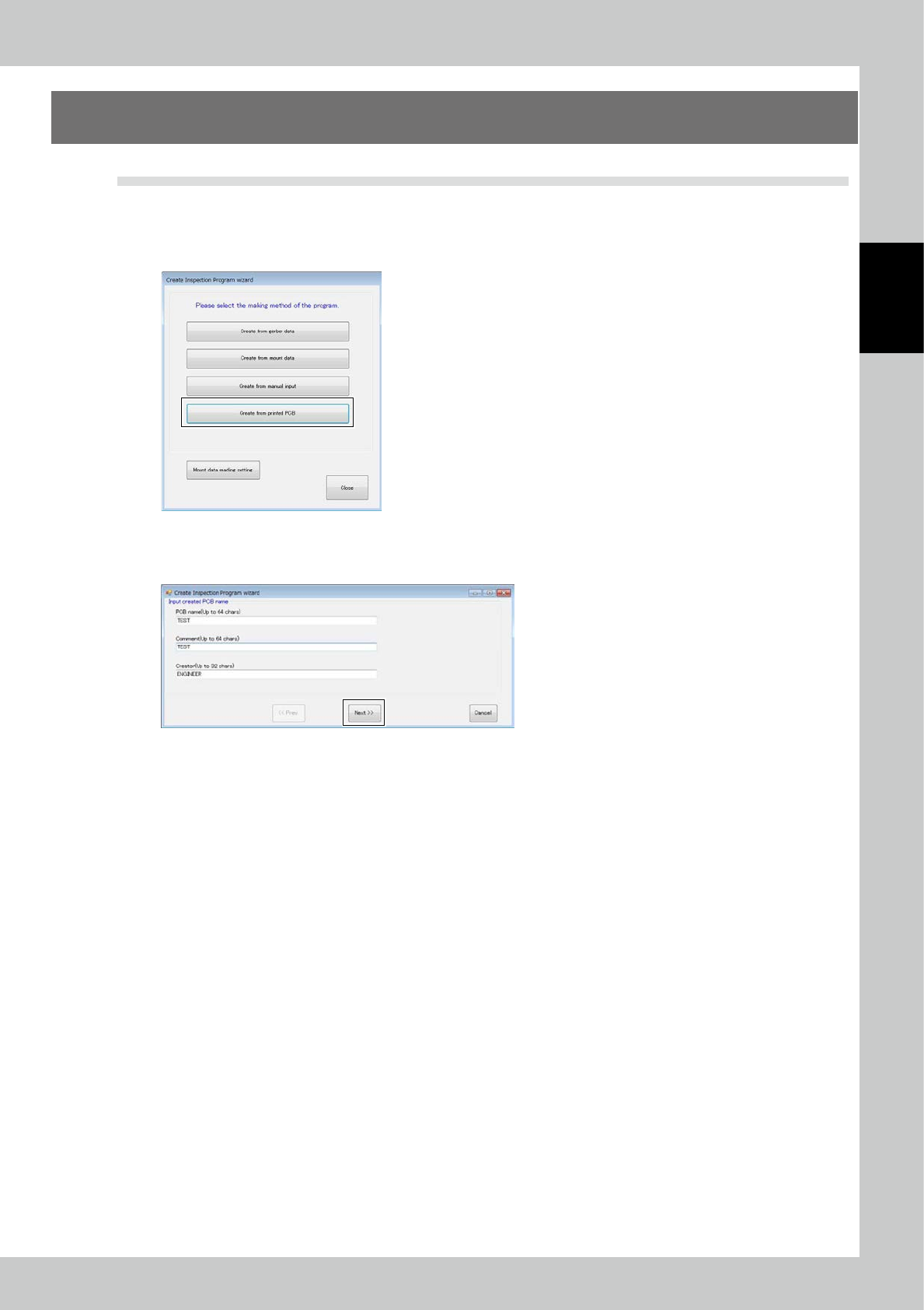
1. Pad extraction
Touch the spec data [Edit] button on the engineer mode screen. The figure shown below is displayed.
24279-KMN-00
Select Printed PCB and click on the [Next] button.
Enter the PCB name and click on the [Next] button.
24280-KMN-00
2-60
2
Operation
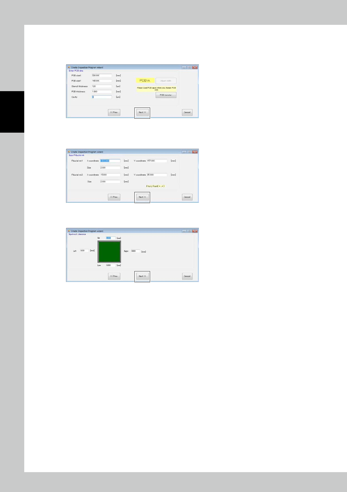
Enter dimension of PCB and thickness of metal mask.
Repeat the step to choose a width setting if required.
Convey PCBs to take them in the machine.
Click the [Next] button.
24281-KMN-00
Enter the coordinates and diameter of the fiducial mark. (Values of the previous PCB are already set.) Click on the
[Next] button.
24282-KMN-00
Enter the margins of the PCB where pad extraction is unnecessary. Click on the [Next] button.
24283-KMN-00
2-61
2
Operation
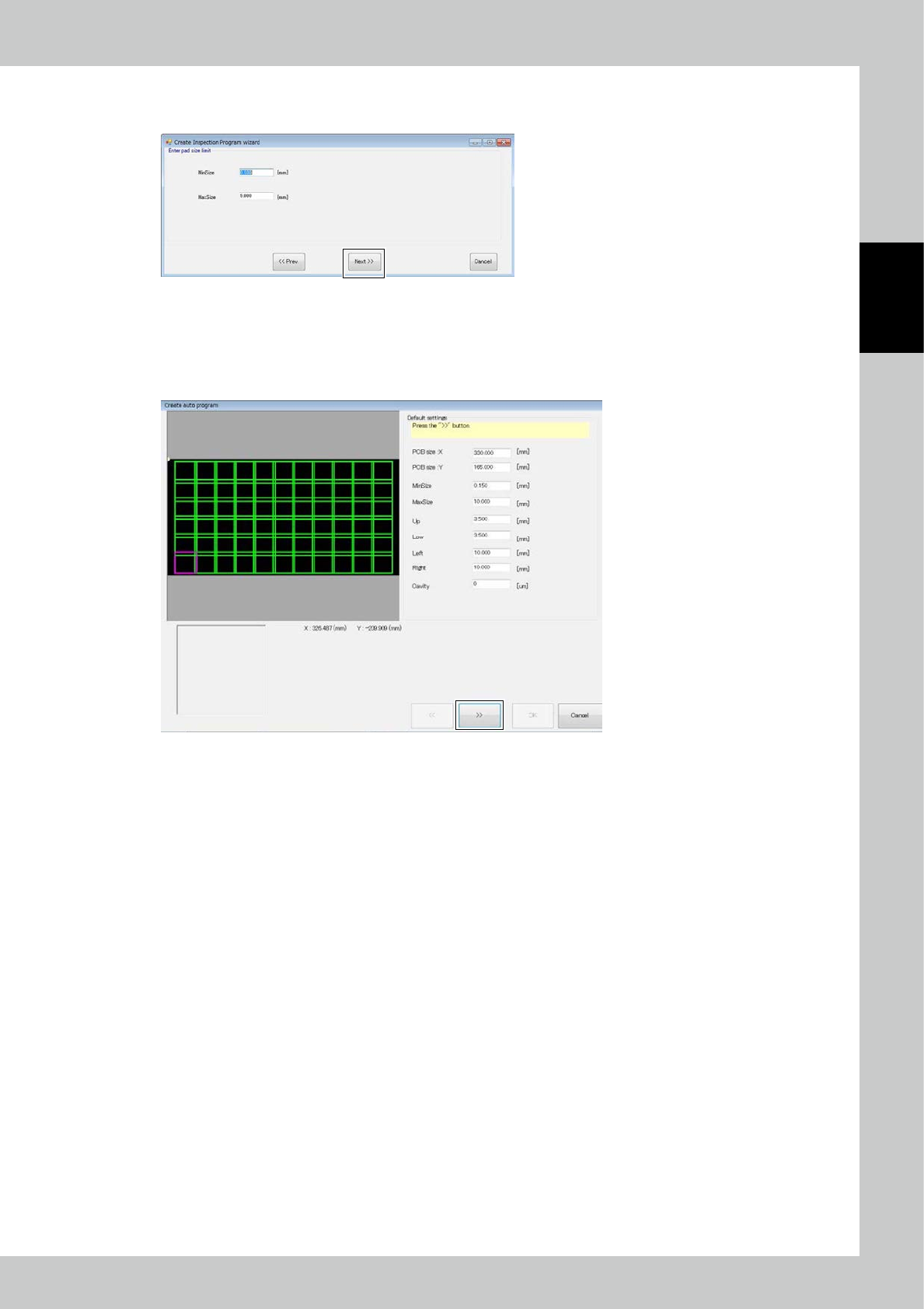
Enter the pad recognition range values.
Click on the [Next] button.
24284-KMN-00
The image of the PCB is displayed. The image shows the pad extraction range and the number of fields of view, based on
the entered PCB data.
The entered values are displayed on the right side of the screen. You can modify values to adjust the PCB image.
After confirmation or adjustment is finished, click on the [>>] button.
24285-KMN-00