YSi-SP_Ope_E.pdf - 第122页
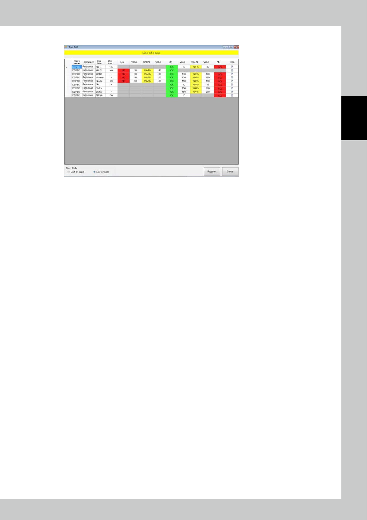
2-85 2 Operation 6. Select List of spec to sho w a spec list. 242B9-KMN-00
2-84
2
Operation
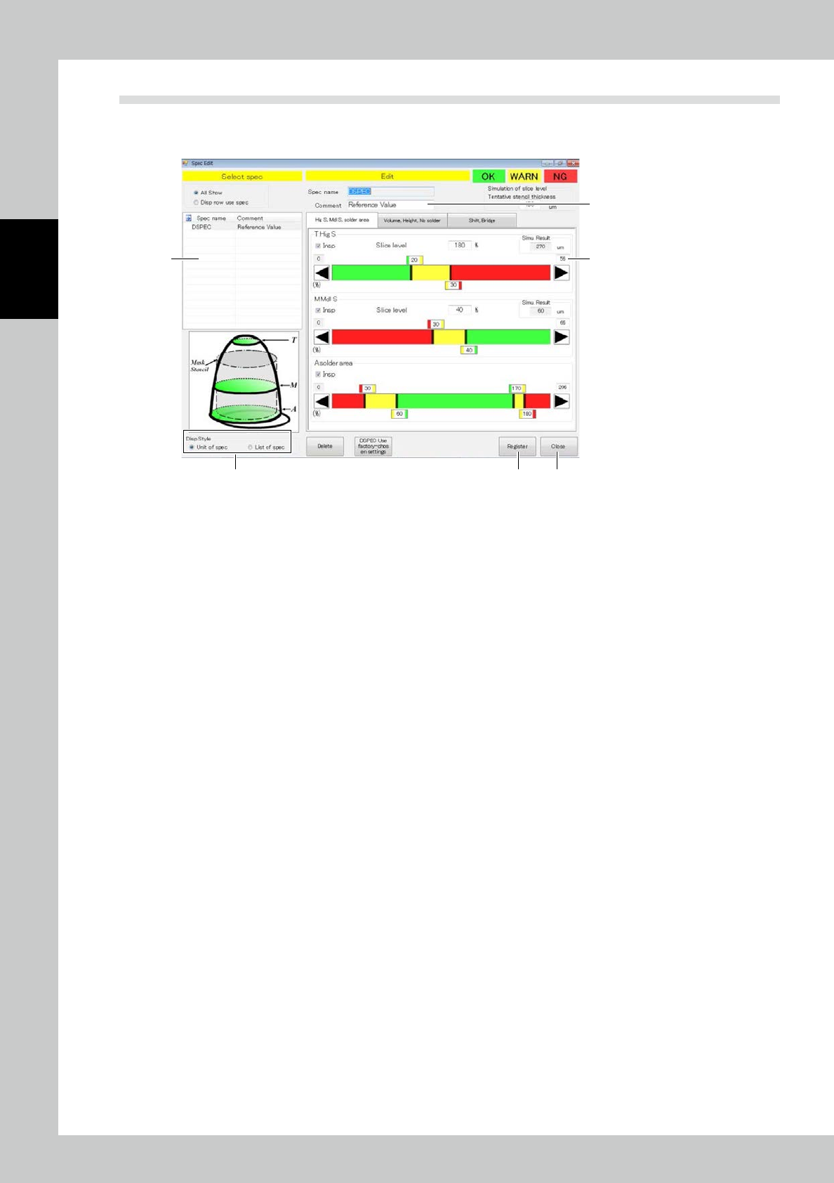
4.3 Spec Data Editing
Edit the spec data.
Touch spec data [Edit] button on the engineer mode screen to display the figure shown below.
1
2
3
4 5
6
242B8-KMN-00
1. Select the spec data to be edited.
2. Enter a comment if you need.
3. According to each inspection item, change the inspection reference value. Touch the upper tab to change over
inspection items.
Inspection is made for inspection items marked with a check mark in the inspection check box. Reset the check box of
unnecessary inspection items for efficient inspection.
4. After spec data is edited, touch the [Register] button.
5. After editing is finished, touch the [Exit] button.
Drag the graph color border or touch the desired arrow button to adjust. The graph color indicates OK (green), WARN
(yellow) or NG (red). Enter the slicing height to the mask thickness in percent directly. For value entry method, refer to
Appendix 2 of the Data Station Volume.
2-85
2
Operation
6. Select List of spec to show a spec list.
242B9-KMN-00
2-86
2
Operation
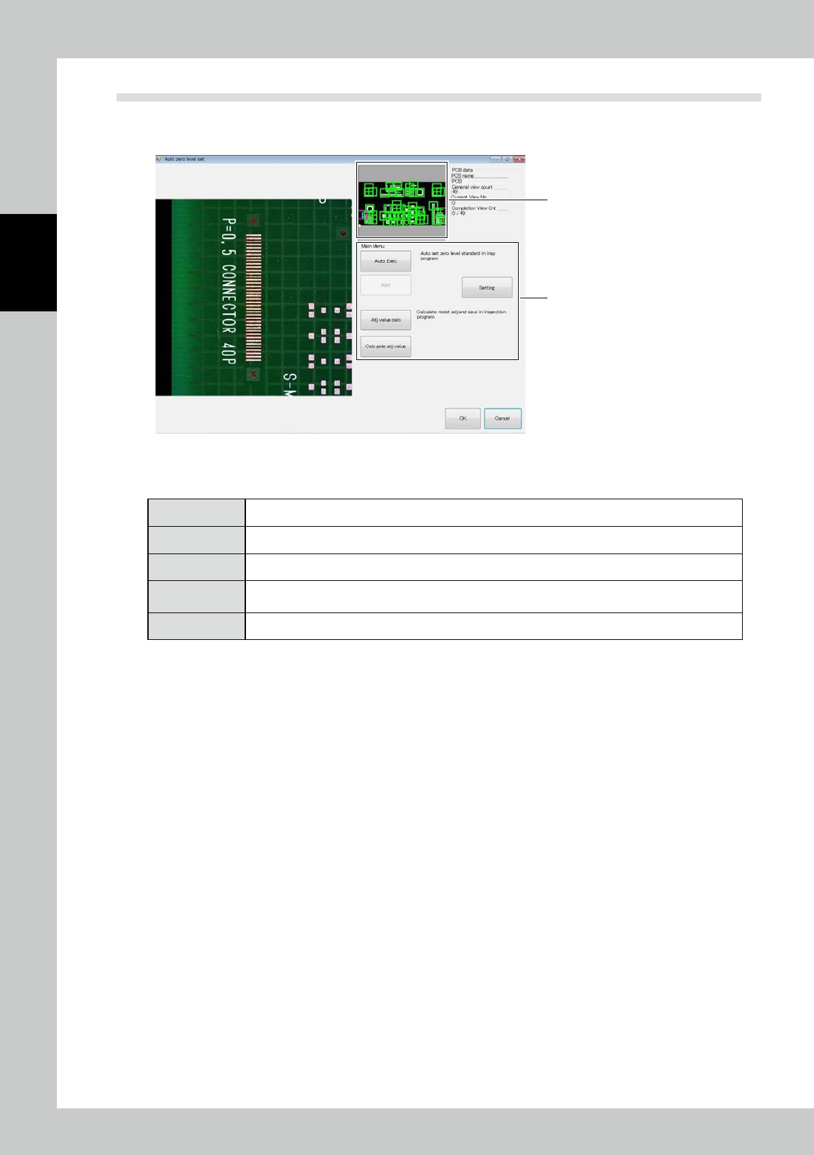
4.4 Automatic Zero Level Setting
Touch the PCB data [Auto zero level setting] button on the engineer mode screen. The screen shown below is
displayed.
2
1
242C0-KMN-00
1. Touch the frame of the field of view to jump to the field of view.
2. "Automatic zero level setting" includes the following menus.
[Auto Exec] The zero level is arranged in all fields of view according to the current extraction setting.
[Adj value calc] The offset of the resist is manually calculated and saved in the inspection program.
[Abrt] Automatic execution is canceled.
[Setting]
Check the settings such as the electrode, silk cut and pattern and resist extraction. [Calc pole adj value]
Teaching proceeds with a real PCB so that the solder height above the electrode face is measured.
[Exit] Exit from the automatic zero level setting procedure to return to the engineer mode tab screen.