YSi-SP_Ope_E.pdf - 第45页
2-8 2 Operation 5 T ouch [Y es] to open the window sho wn below . Adjustment is e xecuted. 24205-KMN-00 n NOTE If there is another PCB inside the PCB when the PCB is being changed, the window shown below is displayed. T …
2-7
2
Operation
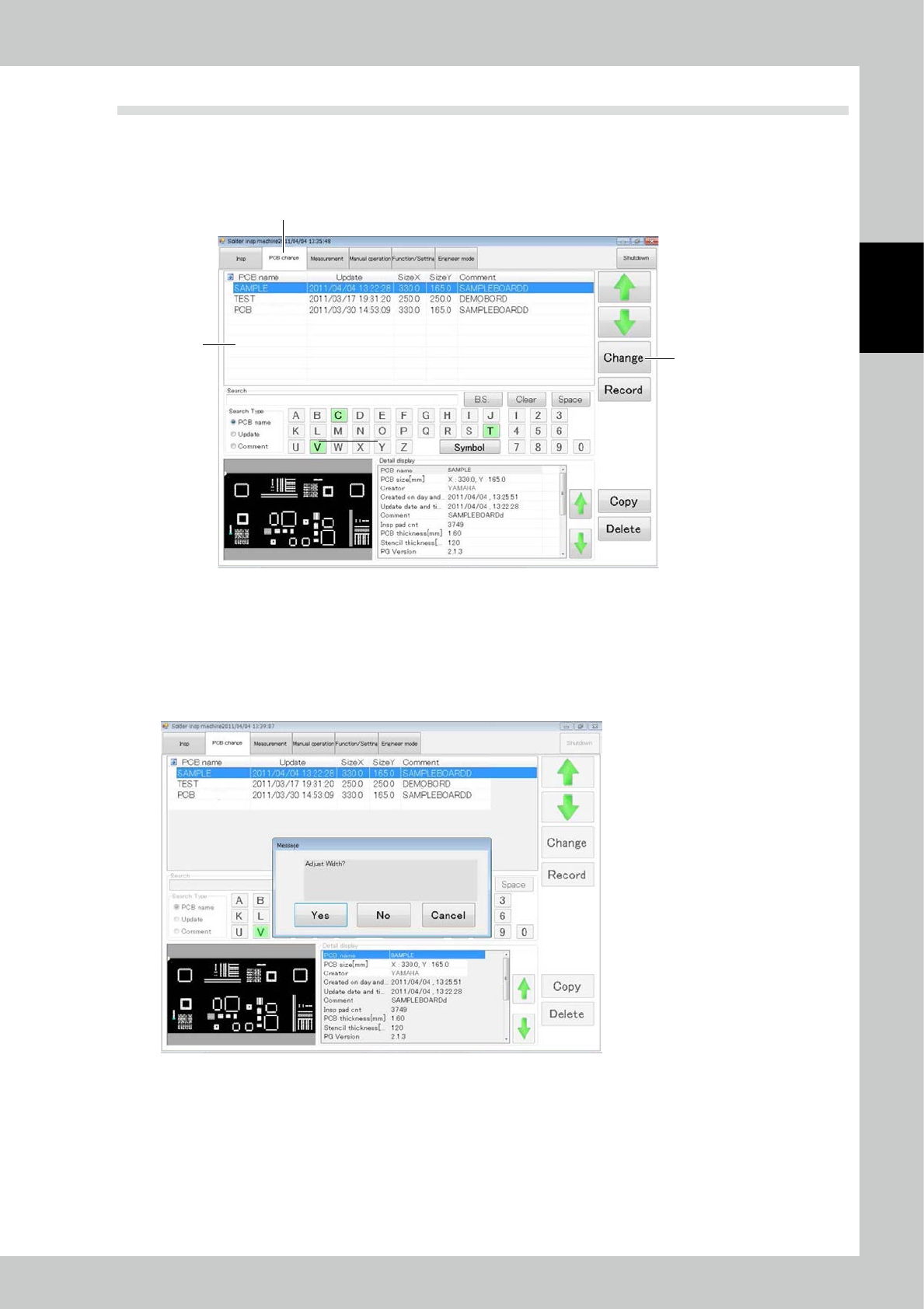
2.4 PCB Change
Select the PCB (inspection program) to be inspected. If there is already a PCB inside the inspection machine,
remove it first. (For the PCB removing method, refer to "2.5.2 Unloading the PCB".)
1
Touch the “PCB change” tab on the main menu screen.
3
2
1
24203-KMN-00
2
The screen shown above is displayed. Select the desired PCB from the list.
3
Touch the [Change] button to change to the selected PCB.
4
After the PCB is changed, the window shown below opens.
Specify whether or not to perform automatic width adjustment during PCB change.
24204-KMN-00
2-8
2
Operation
5
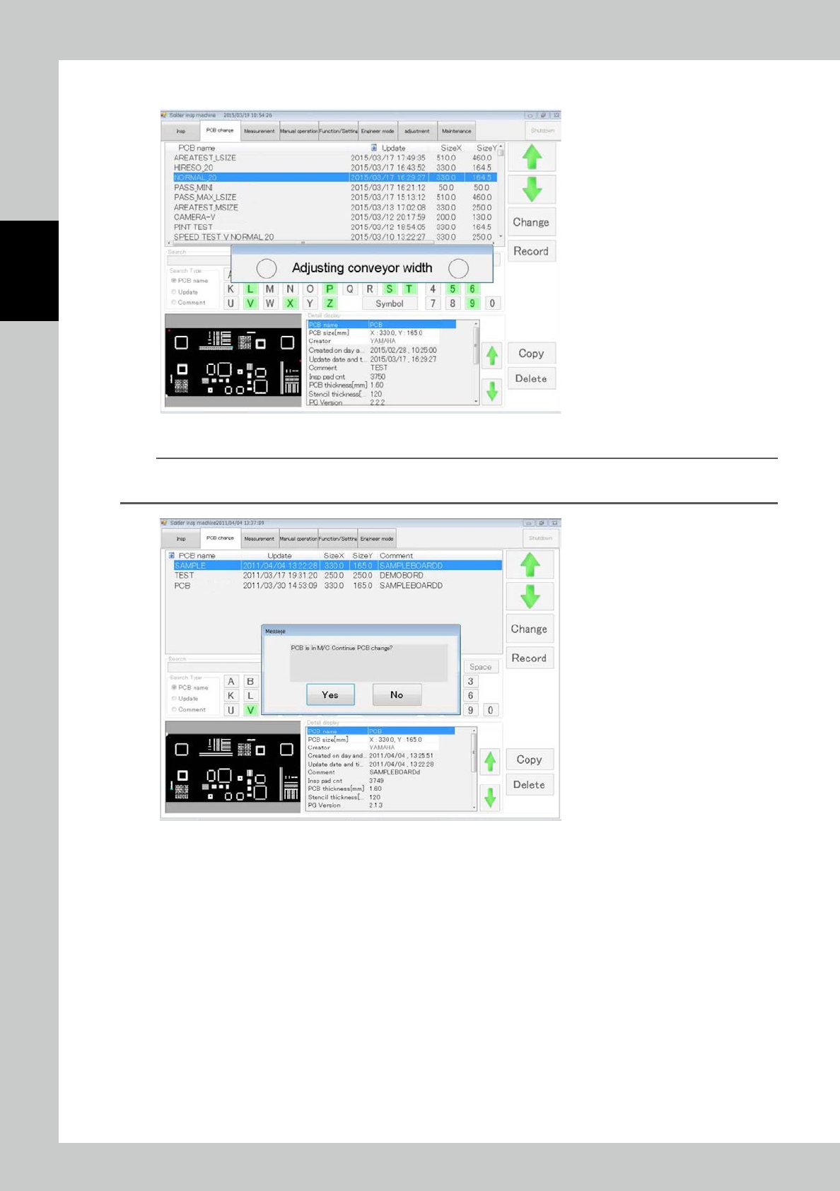
Touch [Yes] to open the window shown below. Adjustment is executed.
24205-KMN-00
n
NOTE
If there is another PCB inside the PCB when the PCB is being changed, the window shown below is displayed. Touch
[Yes] to execute PCB change only without width adjustment.
24206-KMN-00
2-9
2
Operation
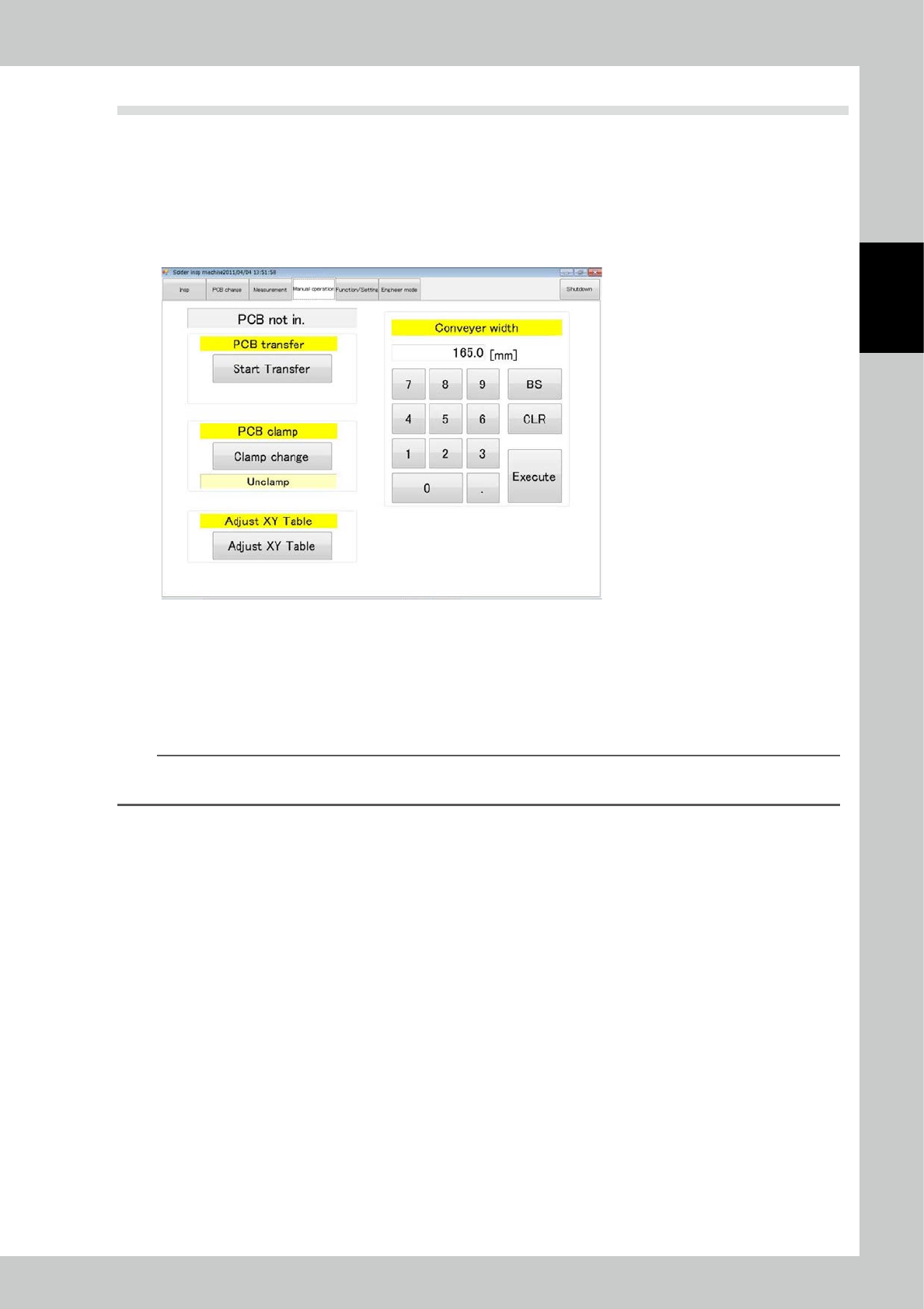
2.5 PCB Transfer
2.5.1 Loading the PCB
After selecting the test piece PCB (inspection program) on the PCB change screen, load the PCB into the
inspection machine. To load the PCB, open the manual operation screen.
1
Touch the manual operation tab on the main menu to open the manual operation
screen.
24207-KMN-00
2
After checking that the PCB has reached the loading port, touch [start transfer].
3
Set the PCB on the rail at the PCB loading port of the inspection machine.
After the PCB is correctly set, a sensor drives the conveyor to move the PCB to the loading port.
4
After being loaded, the PCB is clamped in the inspection machine.
TIP
If the conveyor width has not been adjusted, enter the conveyor width in the conveyor width field on the right side of
the screen before starting to load.
2.5.2 Unloading the PCB
While the PCB is in the machine, touch the [start transfer] button on the manual operation screen (see the
figure above). The PCB is unloaded to the unloading port.