YSi-SP_Ope_E.pdf - 第68页
2-31 2 Operation 2. Displaying the PCB warping measuring result at the menu of “Distr disp”. 24234-KMN-00 3. “Display W arping” button is existed in the tab that is opened by pushing distribution display tab. 4. Displayi…
2-30
2
Operation
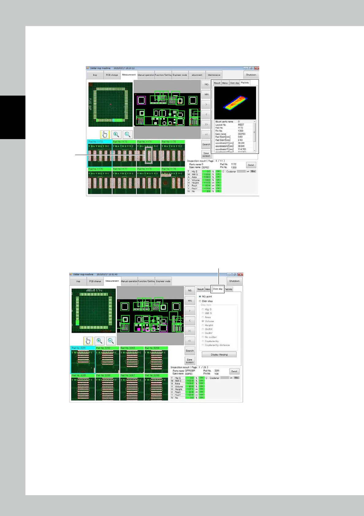
3.4.5 Pad info
The "Pad info" view and each function are described.
The shape of the pad selected at 1 and detail information about the pad can be checked.
1
24232-KMN-00
3.4.6 PCB Warping Measuring Function
The " PCB Warping Measuring Function " view and each function are described.
1. Opening the “Distribution display window” at measuring tab.
At right side of the screen after push the measuring tab, four tabs will be displayed.
Please push the “Distr disp” tab.
Distr disptab
24233-KMN-00
2-31
2
Operation
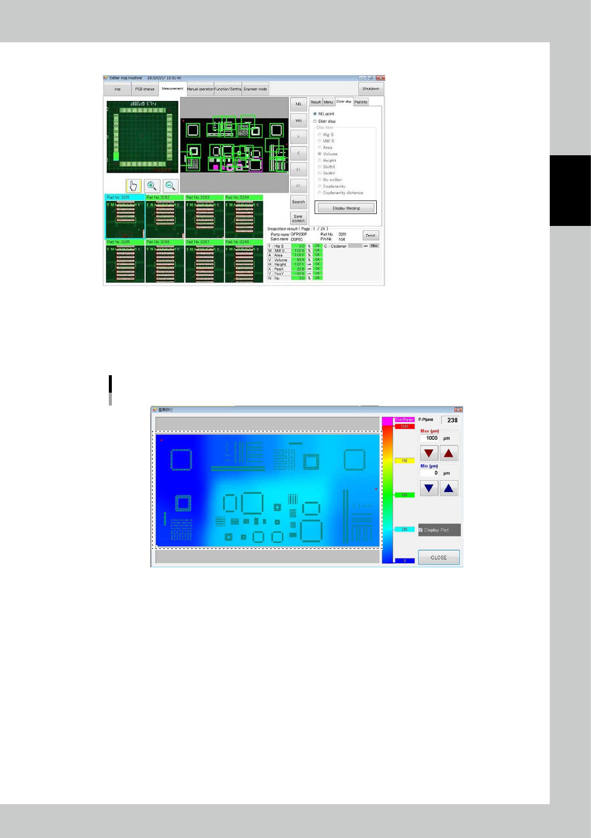
2. Displaying the PCB warping measuring result at the menu of “Distr disp”.
24234-KMN-00
3. “Display Warping” button is existed in the tab that is opened by pushing distribution display tab.
4. Displaying PCB warping measuring result at the menu of “Distr disp”.
PCB warping distribution display part is occupied almost of the window. It is displayed by Variation of colors according
as the level of warping.
Distribution Map
24235-KMN-00
2-32
2
Operation
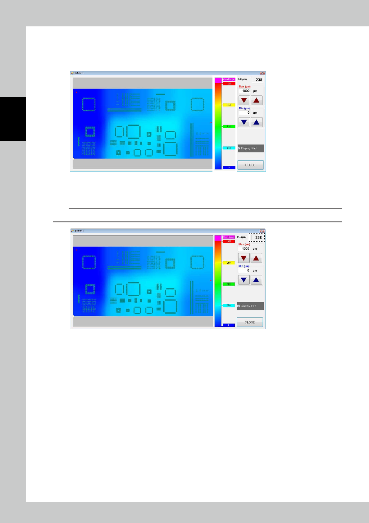
5. Color distribution operating bar (Graduation-Bar)
It is indicated the mutual relation of displaying-color and the level of PCB warping at this bar.
The Values of displaying here is changed according as max value automatically as changing max value of PCB warping
display that we explain in late chapter.
24236-KMN-00
6. Max value of PCB warping display
Max value of whole PCB warping range will be displayed at upper-right of window. (Unit: μ
m
)
TIP
Since it is a reference value, there may be a slight difference from the actual warping value.
24237-KMN-00