YSi-SP_Ope_E.pdf - 第114页
2-77 2 Operation 1. PCB set 2 1 3 242A8-KMN-00 1. T ouch the [PCB set] button. 2. T ouch the [Check] button to acquire the image and show the result on the screen. Check that the end of the PCB is red line. ” 3. T ouch “…
2-76
2
Operation
■
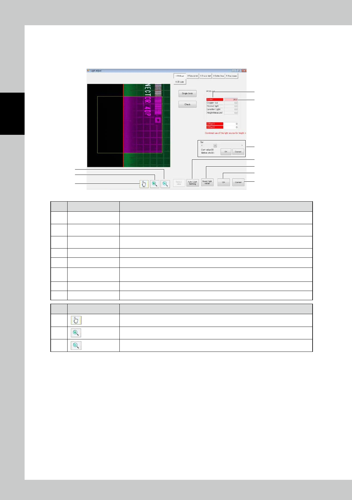
How to adjust the light intensity
To adjust the light intensity, use the table displayed on the right side of the screen during execution of the inspection
menu for light intensity adjustment.
This operation is common for the light intensity adjustment function.
2
1
9
10
11
5
6
7
8
3
242A7-KMN-00
No Name Description of displayed item and functions
1 Light source ON / OFF
ON and OFF alternate each time an item on the left row is touched. The one indicated in red
is turned on, while another indicated in no color is turned off.
2 Light intensity
Touch the number in the right row to highlight the background of the frame in pink, and the
brightness setting panel is displayed below.
3 Brightness setting
Use the scroll bar to adjust the value and press the [OK] button to determine. The setting
range is from 0 to 100%. To refrain from adjustment, touch the [Cancel] button.
4 [Move View] button Move to a designated view.
5 Auto Light Setting Make automatic adjustment of the light intensity.
6
[Reset light value]
button
The current setting becomes the initial value of light intensity. The initial value becomes the
light intensity assigned automatically when new PCB data is created.
7 [OK] button Save the current setting in the selected PCB data.
8 [Cancel] button Exit from light intensity adjustment and return to the engineer screen.
No Name Description of displayed item and functions
9
Cancel the zoom-in/out mode and start the edit mode.
10
Start the zoom-in mode. Touch the screen to enlarge the image around the designated point.
11
Start the zoom-out mode. Touch the screen to reduce the image around the designated point.
2-77
2
Operation
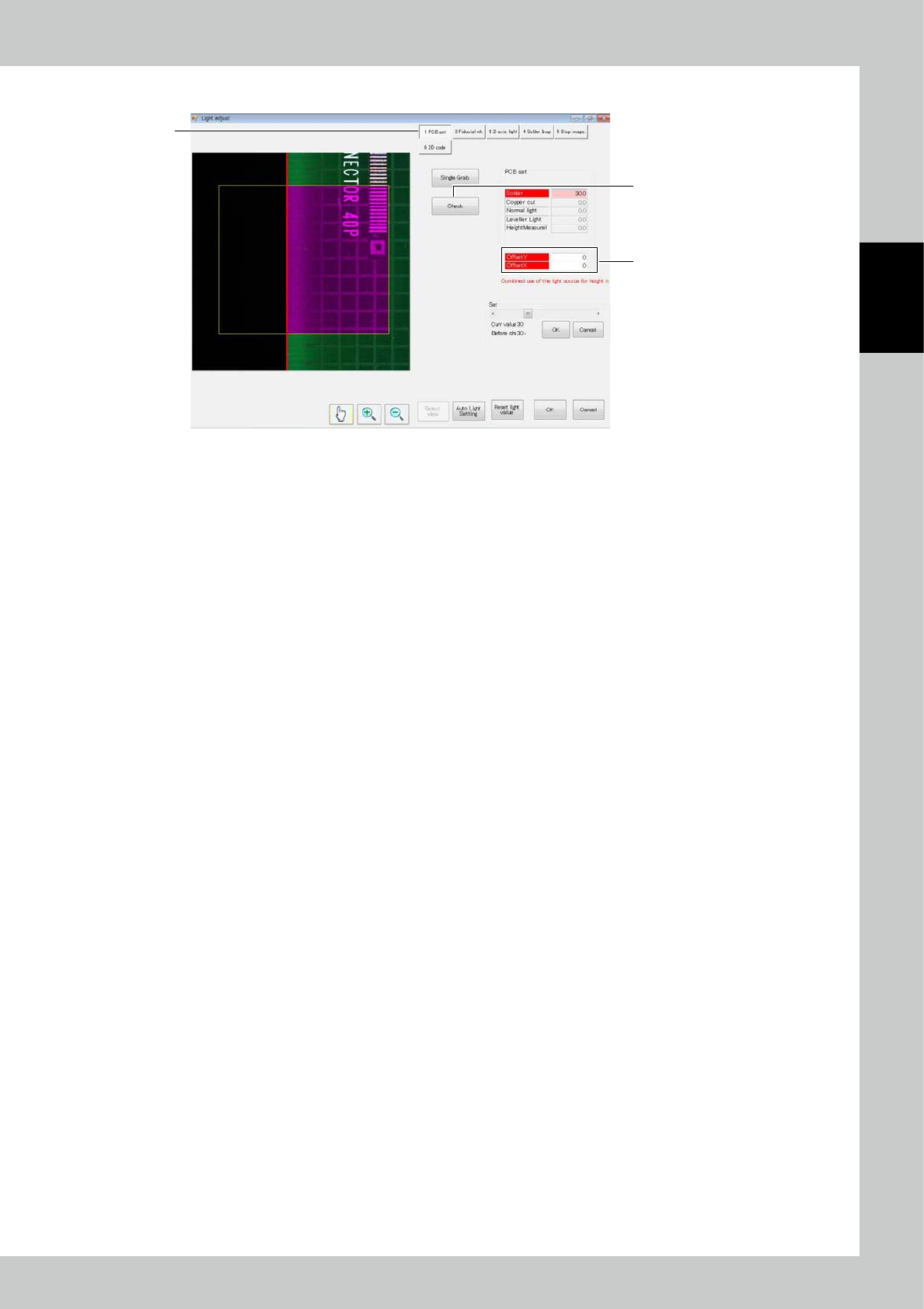
1. PCB set
2
1
3
242A8-KMN-00
1. Touch the [PCB set] button.
2. Touch the [Check] button to acquire the image and show the result on the screen.
Check that the end of the PCB is red line.”
3. Touch “Offset” to adjust the position.
2-78
2
Operation
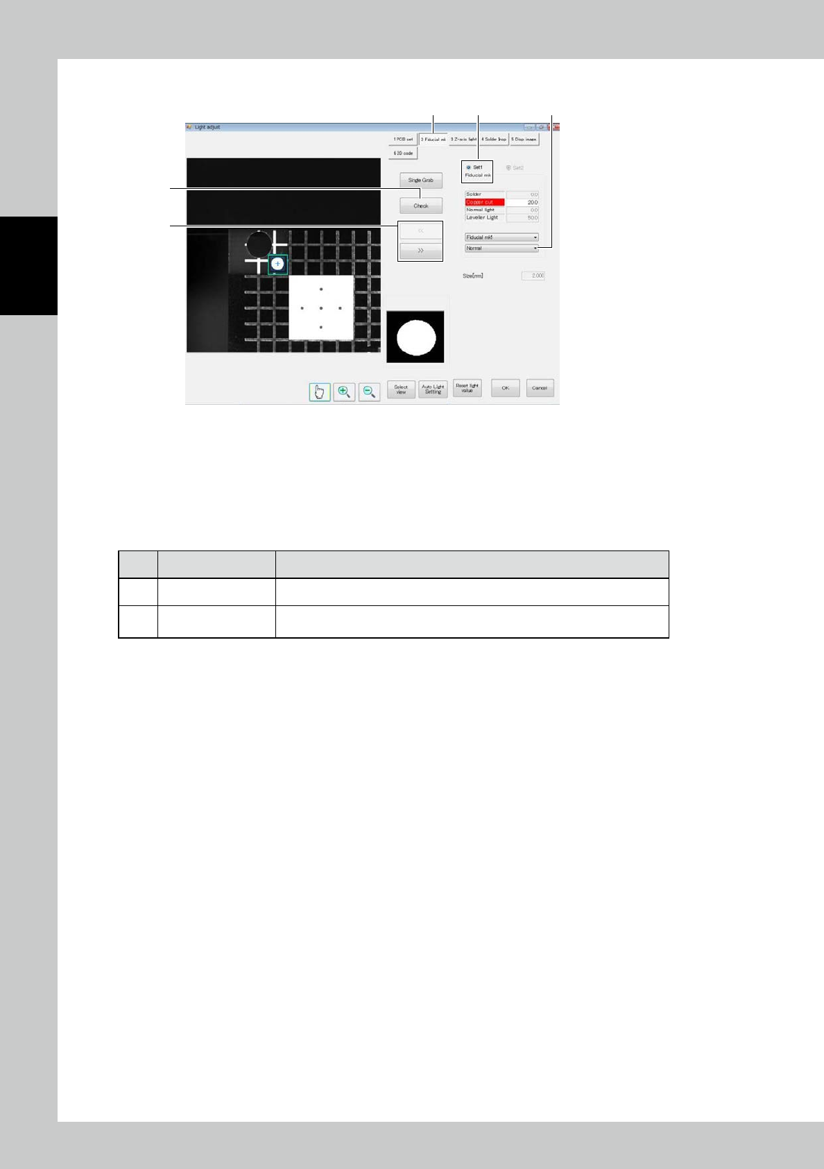
2. Fiducial mark
2
41
3
5
242A9-KMN-00
1. Touch the [Fiducial mk1] button.
2. When the [Check] button is touched, the screen shows the result of check. The reference frame is displayed in white,
while the accurate frame is displayed in blue.
3. Touch the [<<] or [>>] button to switch between fiducial mark 1 and fiducial mark 2, and perform the similar
procedure to adjust.
■
Description of screen
No. Name Displayed data and function
4 Select fiducial mark Enter the setting of the selected fiducial mark.
5
Select judgment
method
Change the fiducial mark judgment method. According to the setting, the
silhouette displayed at the lower right of the screen changes.