YSi-SP_Ope_E.pdf - 第117页
2-80 2 Operation 5. 3D inspection 3 4 1 2 242B2-KMN-00 1. T ouch the 3D Inspection Button. F or a start, adjust the first light projector . T ouch the [3D inspection] button. 2. T ouch the [<<] or [>>] button…
2-79
2
Operation
3. Normal image
2
1
3
242B0-KMN-00
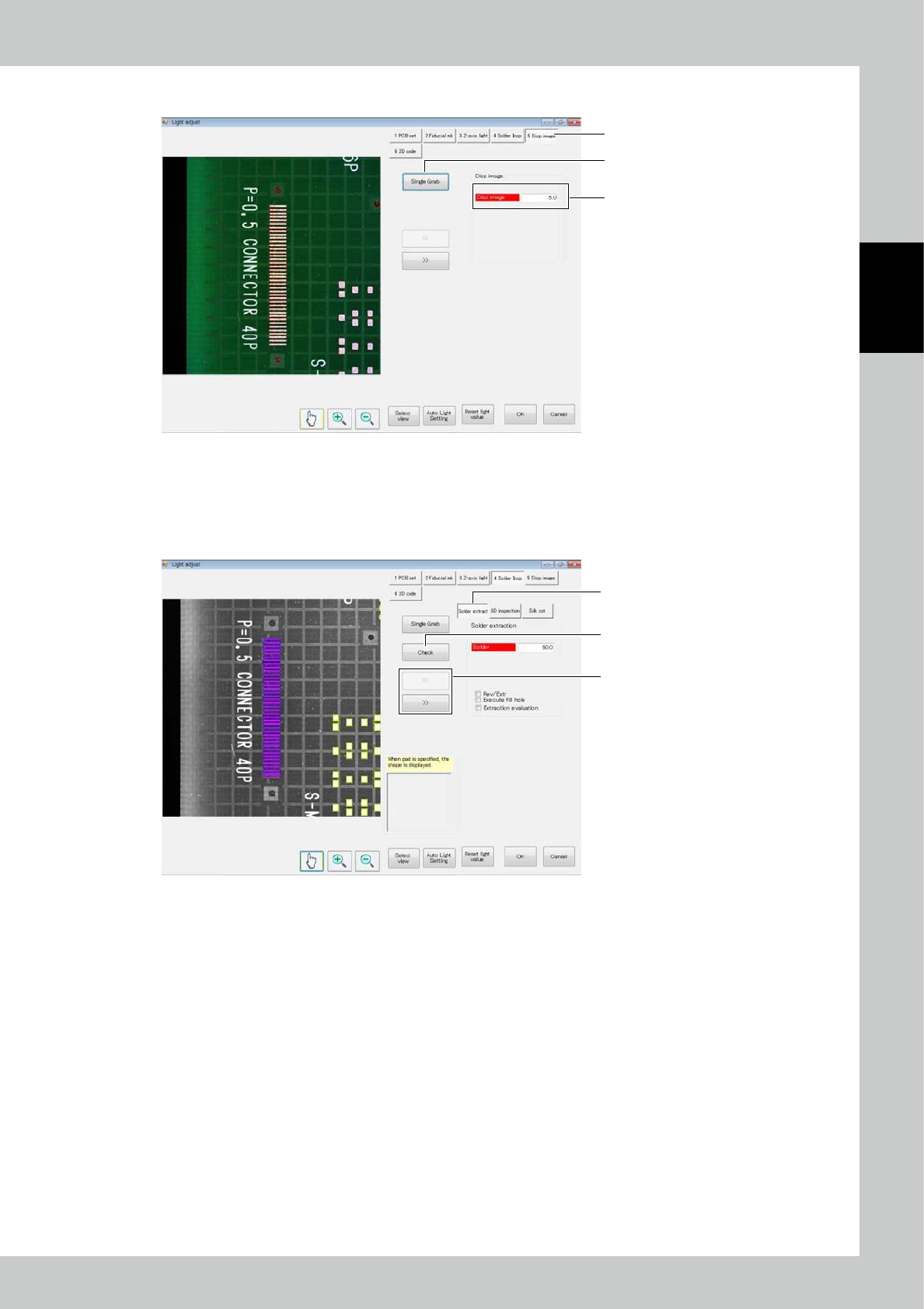
1. Touch the [Dsp image] button.
2. Touch the [Single Grab] button to refresh the image.
3. Change the normal light source value to change the brightness of the image.
4. Solder extraction
1
3
2
242B1-KMN-00
1. Touch the [Solder Insp] button. Touch the [Solder extraction] button.
2. Touch the [<<] or [>> button to select the field of view.
3. Touch the [Check] button to display the results of check on the screen.
2-80
2
Operation
5. 3D inspection
3
4
1
2
242B2-KMN-00
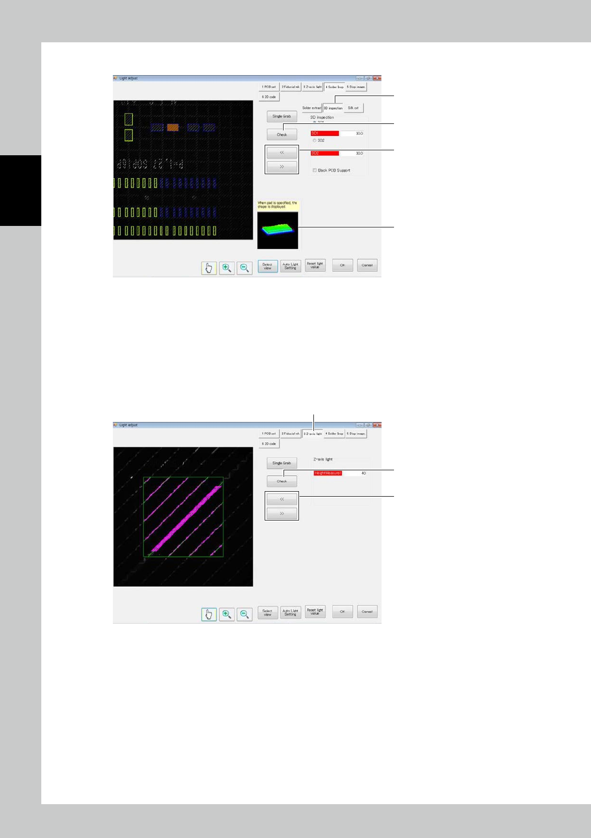
1. Touch the 3D Inspection Button. For a start, adjust the first light projector. Touch the [3D inspection] button.
2. Touch the [<<] or [>>] button to select the field of view.
3. Touch the [Check] button to display the results of check on the screen. The color gradation helps recognize the height
variation.
For height check, zero levels must be defined.
To check the height, define the zero level first.
4. After checking, select a pad in the field of view image to show the shape of the designated point.
6. Z-axis light source
3
1
2
242B3-KMN-00
1. Touch the [Z-axis light] button.
2. Touch the [<<] or [>] button to select the field of view.
3. Touch the [Check] button to display the results on the screen.
Checks whether extracted along the stripe.
2-81
2
Operation
7. Silk cut
3
5
1
2
4
242B4-KMN-00
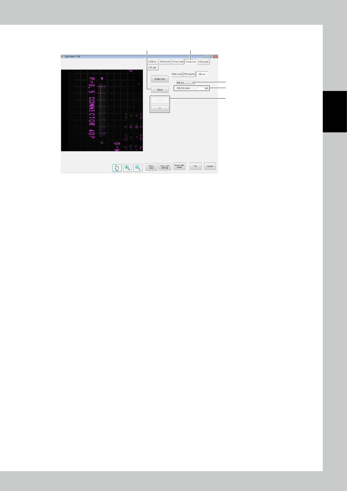
1. Touch the [Solder Insp] button. Touch the [Silk Cut] button.
2. Touch the [<<] or [>>] button to select the field of view.
3. Touch the [Check] button to display the result on the screen.
Check whether the silk part of the PCB and the exposure part of the electrode turn to pink color.
The pink colored part is the part which shall be silk-cut.
4. Adjust the [Silk Cut Level] so that the silk part becomes pink.
5. To invalidate silk cutting, select [No insp].