MV-9_Chapter 5. Teaching.pdf - 第106页
MV -9 Use r Manual 5- 106 5.3.6 IC/Bridge inspection window - IC/Bridge inspection is an al gor i thm to detect defe ct that occurs at l ead p art of IC com ponen t. judge whether there is bridg e bet ween lead and defec…
错误!使用“开始”选项卡将 제목 2 应用于要在此处显示的文字。错误!使用“开始”选项卡将 제목 2 应用
于要在此处显示的文字。 .
5-105
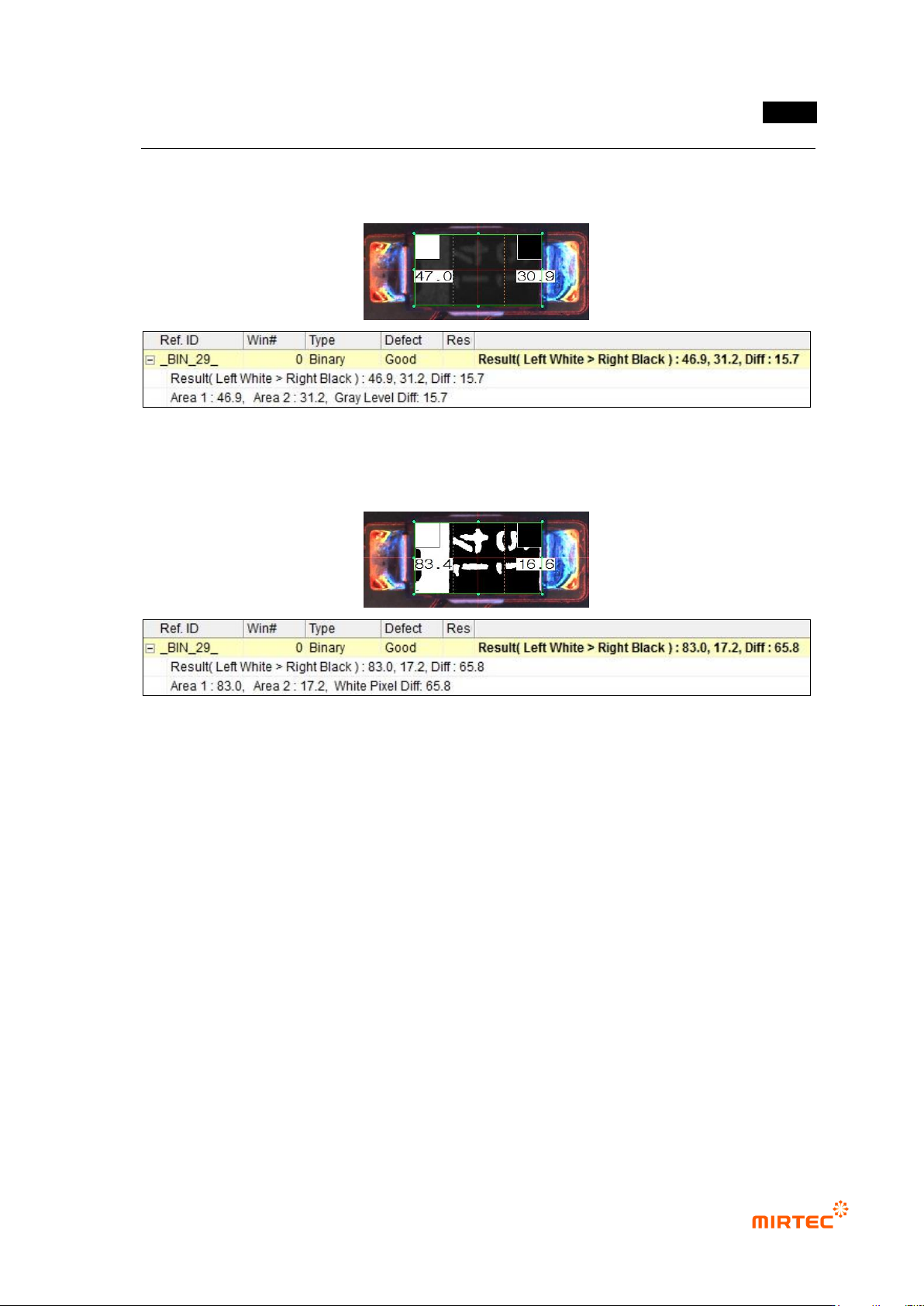
Luminance comparison
[Figure 5-110 luminance comparison inspection result]
Pixel comparison
[Figure 5-111 Luminance comparison inspection result]
MV-9 User Manual
5-106
5.3.6 IC/Bridge inspection window
- IC/Bridge inspection is an algorithm to detect defect that occurs at lead part of IC
component. judge whether there is bridge between lead and defect of soldering status of
each lead end. this system sets one inspection area to inspect various errors that occurs
at lead part of IC component to increase users‟ operational convenience and the system
has detailed adjustment items for inspection to raise inspection reliability.
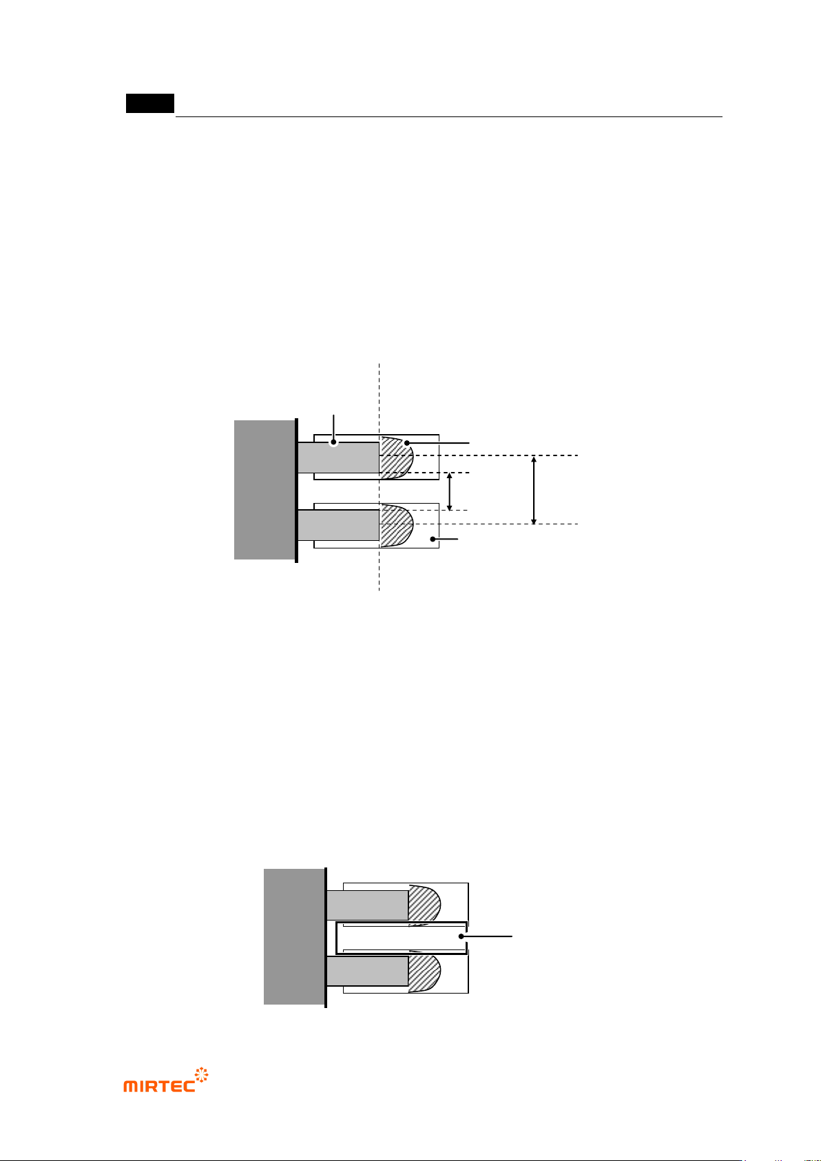
1) Definition of each area of IC lead
[Figure 5-112 IC lead part]
Bridge defect
- In case of normal (no defect), solder must exist only on pad area that fixes IC lead.
However, in case of a defect, solder on the pad pushed out into gap area between lead
and connect both lead. This is called as Bridge defect.
- To detect this defect, solder in gap area must be checked to inspect IC lead. Hence, judge
bridge defect by checking binarization of image from camera and distribution shape of
white pixel in gap area.
- this system conducts separate lead separation before inspection to increase bridge
inspection performance and use separate and Bridge inspection for separated gap area.
Inspection area
Lead end
Solder Fillet
Lead
Pitch
Gap
Pad
错误!使用“开始”选项卡将 제목 2 应用于要在此处显示的文字。错误!使用“开始”选项卡将 제목 2 应用
于要在此处显示的文字。 .
5-107
[Figure 5-113 IC lead Bridge inspection area]
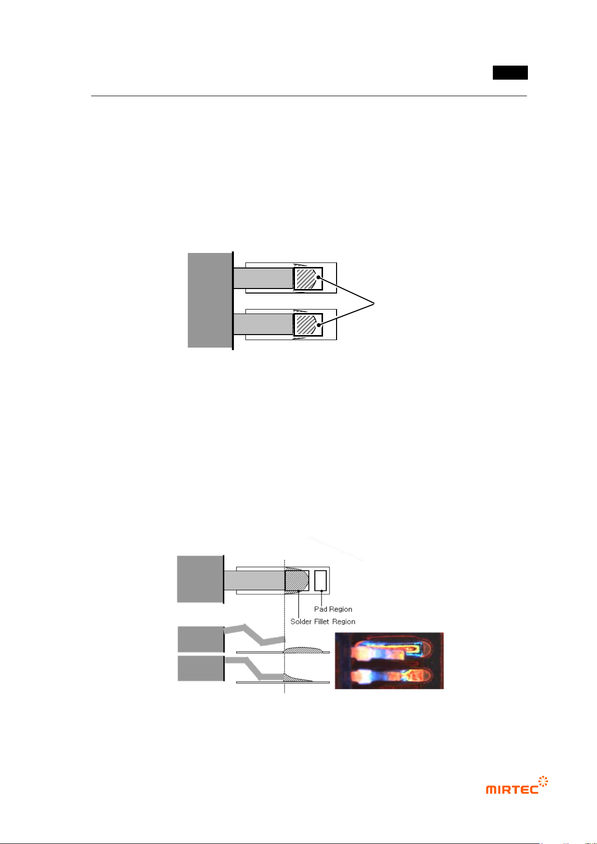
Solder defect
- If reflow is skipped, lead on pad is melt and shows burning shape after IC component is
mounted by mounter. There should be enough amount of lead to fix it on the pad. However,
if screen printer incompletely applies lead, small amount of lead is applied to some pad
area, and there will be problem of fixing of IC component after reflow. This solder defect is
called as no solder or insufficient solder. Therefore, lead amount in solder fillet area must
be inspected to detect solder defect.
- This system uses image that binarized inspection area to judge solder defect.
[Figure 5-114 IC lead solder inspection area]
Lifted defect
- If lead of mounted IC component is vertically bent or one side of component itself is slope
and lifted from substrate during mounting, lead is not soldered on pad. This is called lifted
defect.
- To inspect defect of IC lead, inspect position of lead tip and lead color in lead area, and
inspect solder paste status in solder fillet area and pad area.
- This system judges lifted defect of IC lead using color information and luminance
information in each inspection area.
[Figure 5-115 IC lead lifted inspection area]
Inspection area
역