MV-9_Chapter 5. Teaching.pdf - 第181页
错误 ! 使用“开始” 选项卡将 제목 2 应用于要在此处显示的文字。 错误 ! 使用“开始”选项卡将 제목 2 应用 于要在此处显示的 文字。 . 5- 181 No electrode auto extraction ① El ectrode m i nor axis length : autom ati cally display average value of m i nor axis length of extracte…
MV-9 User Manual
5-180
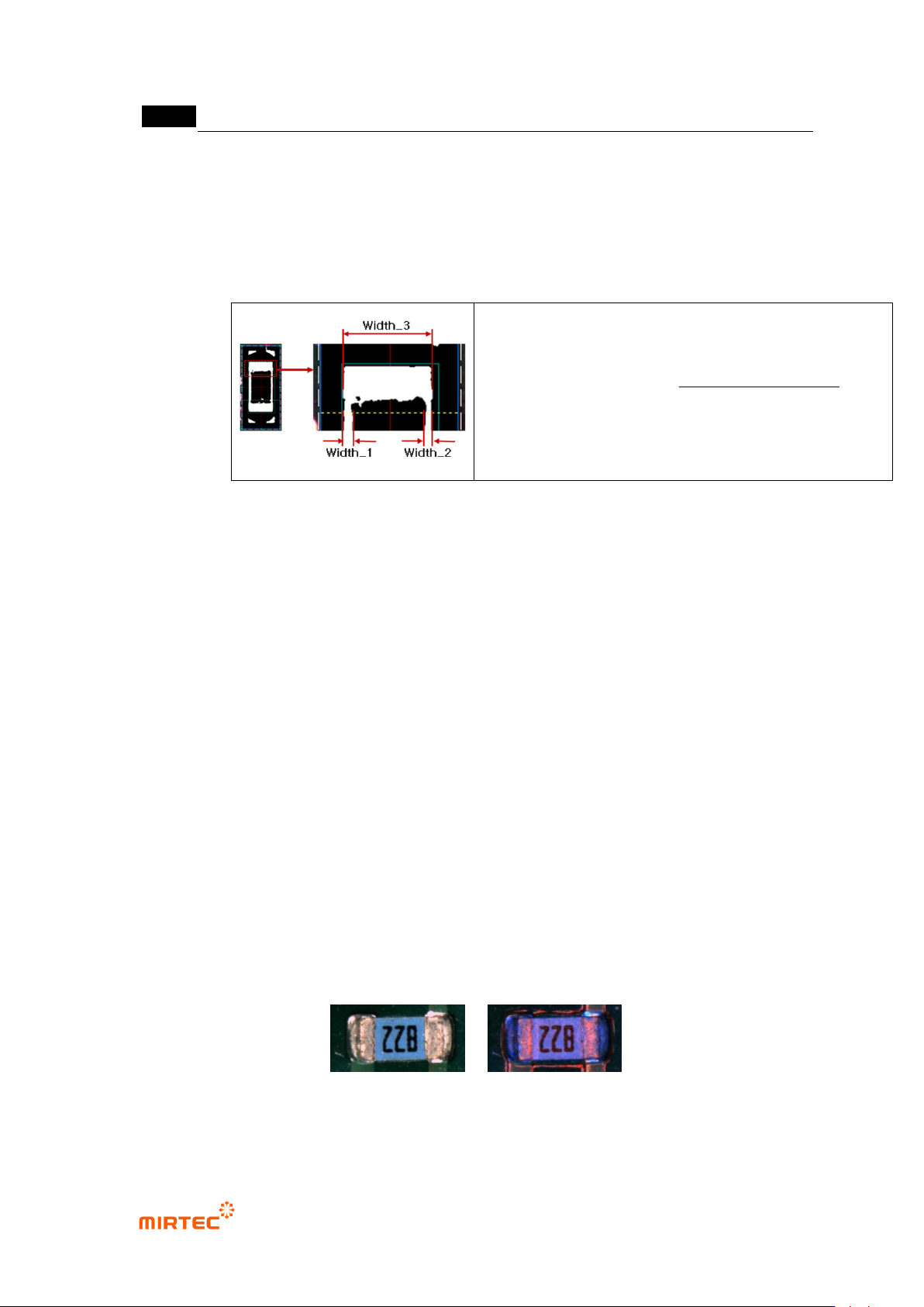
- This is to extract electrode only. Check at the button to remove body edge component and
to find electrode. At this point, width of edge to be removed is below certain ratio of
electrode width, remove it. The following is calculation formula of width ratio. As shown in
[Figure 5-164], Width_1 and Width_2 is the width of silk to be removed, Width_3 is the
width electrode.
100
Width_3
Width_2)(Width_1
(%)edit width electrode
[Figure 5-221 noise removal – definition of electrode edit width]
Chip Info
① Chip Type
- This will be automatically set in optimization stage, and judge and display chip model that
completed teaching using size of mounting window.
② Special chip
- If the body area of chip to be inspected is displayed in blue (In case of component of which
chip body is blue), check special chip, select color map-pad on [pad inspection] tap, and
then adjust color map to display chip body area in blue.
- In general, Manhattan and Tomb Stone of normal C chip is judged based on the fact that
body area is red. In case of normal R chip, judged based on the fact that body area is
black, and in case of chip color algorithm, judged based on blue ratio in chip body area.
Chip of which chip body is blue will be judged as defect under these judgment criteria.
Therefore, special chip setting is special condition to reduce false defect.
- In case of setting a special chip, if blue ratio in chip body area is lower than reference
value that is set inside (user change is impossible based on 1/3 of other area excluding
electrode on chip), judge as defect.
(Horizontal image) (Color image)
[Figure 5-222 Example of chip of which chip body area is blue]
错误!使用“开始”选项卡将 제목 2 应用于要在此处显示的文字。错误!使用“开始”选项卡将 제목 2 应用
于要在此处显示的文字。 .
5-181
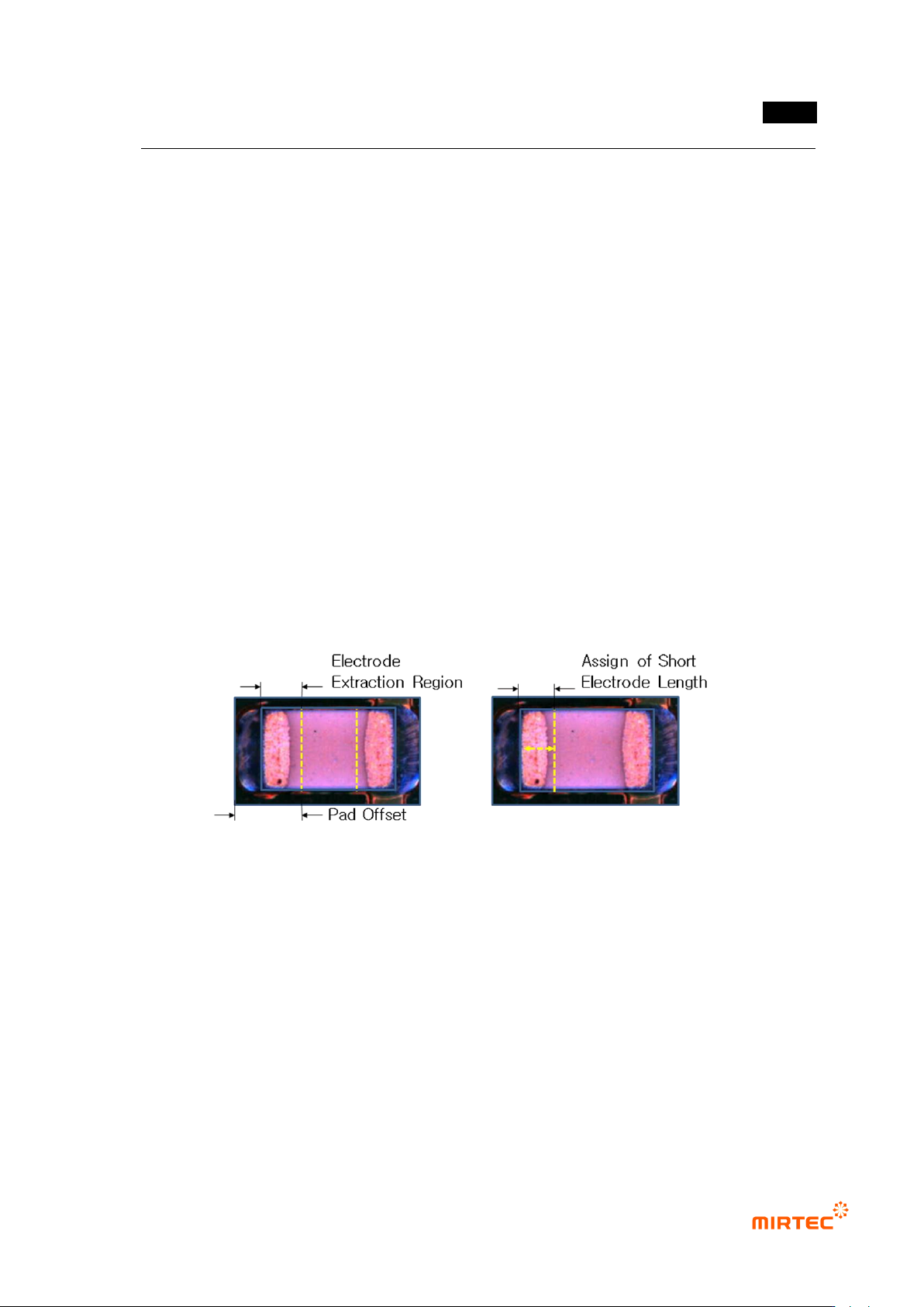
No electrode auto extraction
① Electrode minor axis length: automatically display average value of minor axis length of
extracted 2 electrodes.
② Electrode major axis length: automatically display average value of major axis length of
extracted 2 electrodes.
- Extract 2 electrode areas after auto binarization in optimization process, and display each
average value of minor axis length and major axis length of 2 electrodes as electrode
minor axis/major axis length.
- body area of chip is displayed in similar luminance and color of electrode and auto
electrode extractions is not possible, check at „Not use electrode auto extraction‟ and
manually adjusts electrode major axis / minor axis length to set electrode area.
- There are 2 methods to manually limit electrode size. the first method is to limit electrode
extraction area using pad offset, and the second method is to check at „Not use electrode
auto extraction‟ and manually set major axis/minor axis length of electrode.
[Figure 5-223 Electrode mounting/minor axis setting method]
- For minor axis length, set area as much as electrode minor axis length set based on
mounting window end as electrode, and set electrode size using trial and error method that
checks the size of inspection area set by conducting trial inspection.
- Major axis/minor axis length of electrode will be based on calculation standard for
electrode color ratio -> short/long size on [pad inspection] tap. In case of C-chip, unusually,
much extraction of electrode occurs. This will make short or long size above 100% in
inspection review to cause false defect. In this case, largely change electrode major
axis/minor axis length value to reduce short/long size ratio. If short size of extracted
MV-9 User Manual
5-182
electrode is 44 and calculated electrode minor axis length is 20 when optimization is
clicked, short size ratio will be calculated to 120%. If minor axis length of electrode is
changed to 23 to set this to max 100%, short size ratio will be reduced down to 91%.
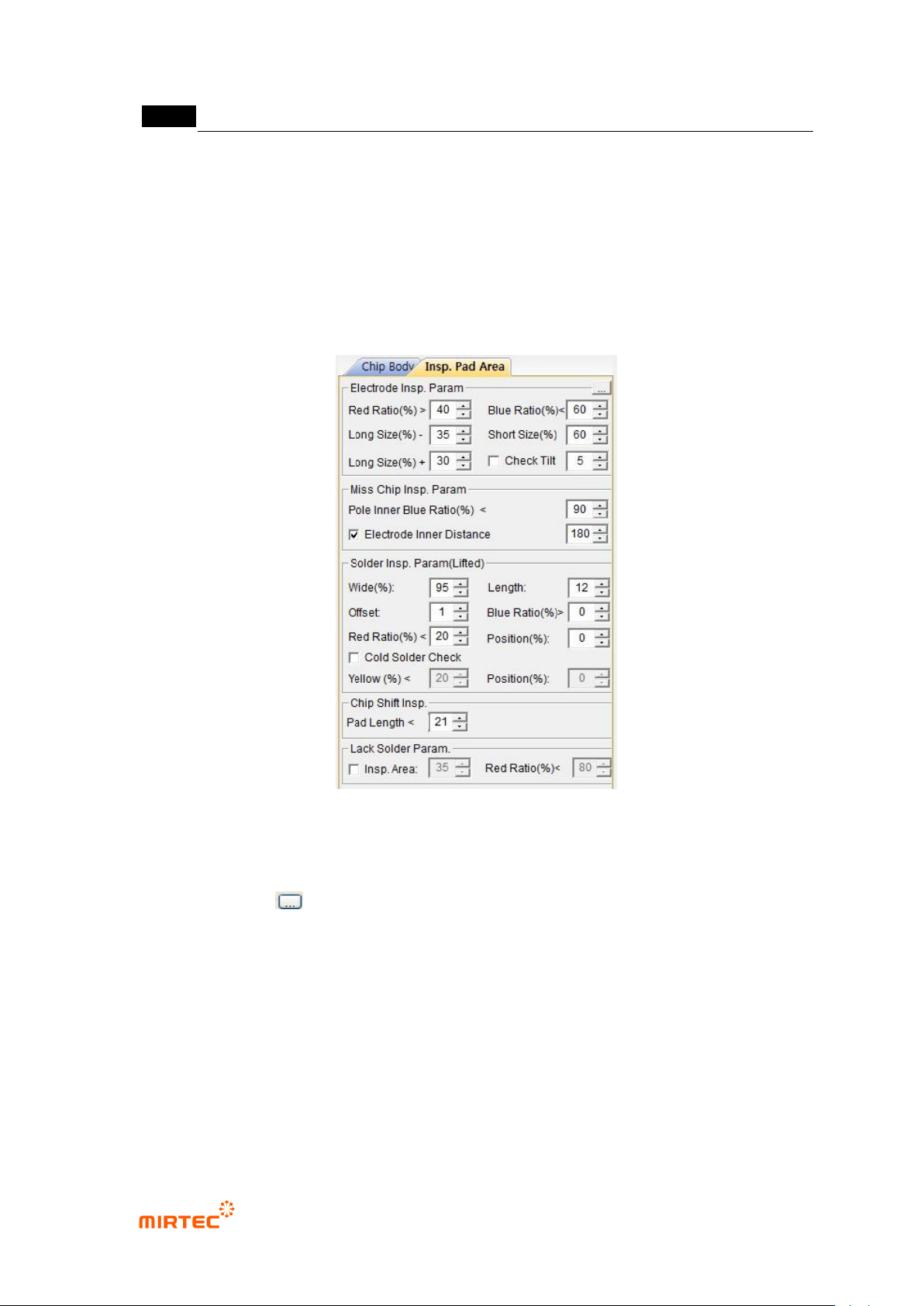
8) Parameter of [pad inspection] tap
- Pad inspection tap is to set criteria for good/defect judgment of chip.
[Figure 5-224 Parameter window of pad extraction tap]
Adjusting color map for inspection
- Click button to conduct binarization based on color map.
① Binarization for pad inspection
- Each of Electrode (electrode), Pad (pad) and Cold Solder can be selected for binarization.
- color map shows hue and saturation of red, green, and blue, and set area for each color to
extract desired color and saturation.
- Right bar is to set min value and max value of area for the color luminance. The method is
same with the adjustment of binarization value for the gray image of existing algorithm.
② Color type