MV-9_Chapter 5. Teaching.pdf - 第56页
MV -9 Use r Manual 5- 56 ⑦ Draw col or inspect i on or solder i nspection w i n dow at the cente r of the p ad for perfora t i on inspe c tion , adjust co l or m ap and b i nar i zation value, and select norm a l judgmen…
错误!使用“开始”选项卡将 제목 2 应用于要在此处显示的文字。错误!使用“开始”选项卡将 제목 2 应用
于要在此处显示的文字。 .
5-55
5.3.3.3. Wave Solder inspection
- Algorithm to inspect soldering status for wave soldering that is a soldering process for
manual mounting or auto mounting soldering component. The inspection is divided into pin
type (pin type) and lead type according to component type. In basic defect type, pin is not
exposed, perforation (or defect of hole in solder area due to pin hole, wettability defect).
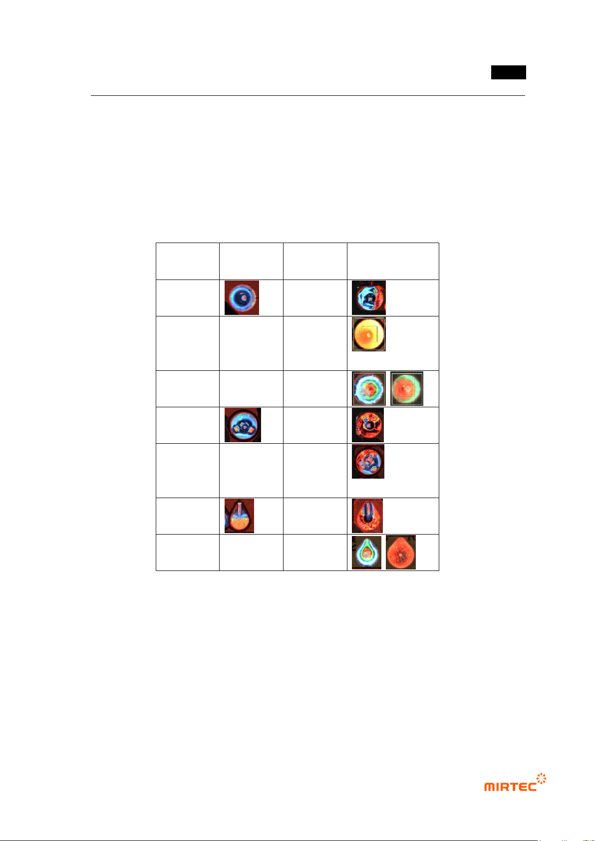
[Table 5-4 4 Binarization methods of solder amount inspection window]
Type
Normal
image
Defect
name
Defect image
pin type
perforation
No solder,
insufficient
solder
no pin
exposure
perforation
No solder,
insufficient
solder
lead type
perforation
no pin
exposure
1) Teaching method
① Click <soldering inspection window> button among operating buttons.
② Draw inspection window in solder area.
③ Select horizontal + vertical light for light type. Image type will be automatically selected.
④ Adjust position and size of pin inspection area and solder inspection area.
⑤ Adjust color map and binarization value checking preview.
⑥ Enter inspection criteria.
MV-9 User Manual
5-56
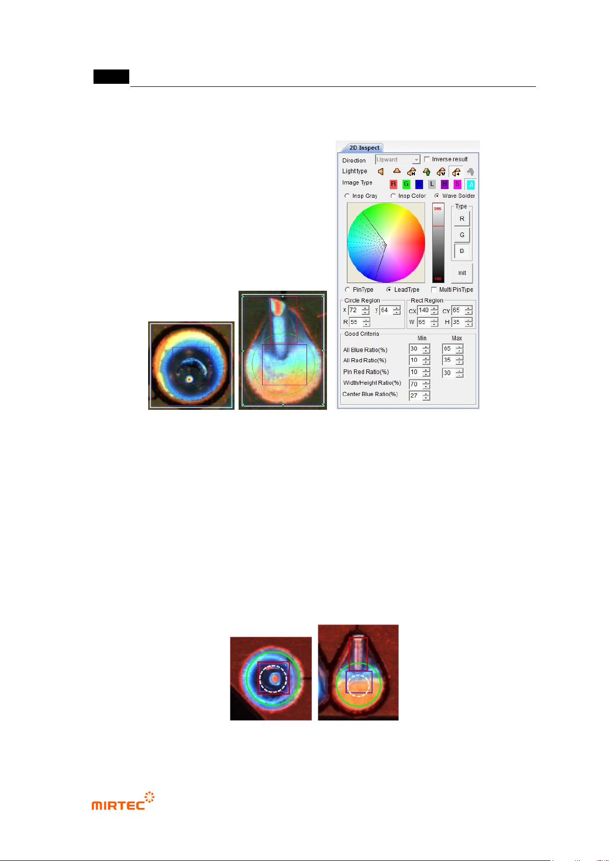
⑦ Draw color inspection or solder inspection window at the center of the pad for perforation
inspection, adjust color map and binarization value, and select normal judgment for defect.
[Figure 5-60 Soldering inspection – wave soldering inspection window creation screen]
2) Teaching example of representative component
- Draw soldering inspection window in wave solder area and select wave solder to
automatically create green circle and red rectangle.
- Green circle is to inspect solder area, and red rectangle is area to inspect pin or lead
exposure.
- White dotted line circle in the center is a virtual area that does not actually appears, and it
is an area to inspect excessive solder. Center of white dotted line circle is same with green
circle, and radius is half of green circle.
- Violet rectangle is an area to inspect perforation.
[Figure 5-61 Example of soldering inspection window teaching]
错误!使用“开始”选项卡将 제목 2 应用于要在此处显示的文字。错误!使用“开始”选项卡将 제목 2 应用
于要在此处显示的文字。 .
5-57
3) Parameter of Wave Solder inspection window
Reference name
- Refer to „reference name (page) ' in „5.3.1
- ‟ excepting shape.
- Created in „_SLD_1_‟ format. At this point, „SLD‟ means Solder and the number means the
creation order of solder amount inspection window.
Component name
- Refer to „component name (page)‟ in „5.3.1 Light type
- Select horizontal + vertical light for wave soldering inspection.
Image type
- Select „A‟ for image type.
Inspection type
- Select wave solder among 3 soldering inspection types.
Component type
- Component type is divided into pin type and lead type according to component. Especially,
in case of pin type, component with one pin is out and component with many pins out. In
case of the second, select Multi Pin Type.
Circle Region
- Designate position and radius of green circle for soldering inspection.
Rect Region
- Designate position of red rectangle and size of width and height to inspect pin lead
exposure.
Good Criteria
- All Blue Ratio (%): blue ratio in green circle area
- All Red Ratio (%): red ratio in green circle area
- Pin Red Ratio (%): red ratio in red rectangle area
- Width / Height Ratio (%): width height width ratio of red area in green circle area
- Center Blue Ratio (%):blue ratio in white circle area