MV-9_Chapter 5. Teaching.pdf - 第80页
MV -9 Use r Manual 5- 80 T o detect Solder ball on LED substrate , set binarization v alue to „ 0 ‟ to m ake t ot al inspe c tion window in white in prev i ew . - Size filtering , space filling For detect io n of sol…
错误!使用“开始”选项卡将 제목 2 应用于要在此处显示的文字。错误!使用“开始”选项卡将 제목 2 应用
于要在此处显示的文字。 .
5-79
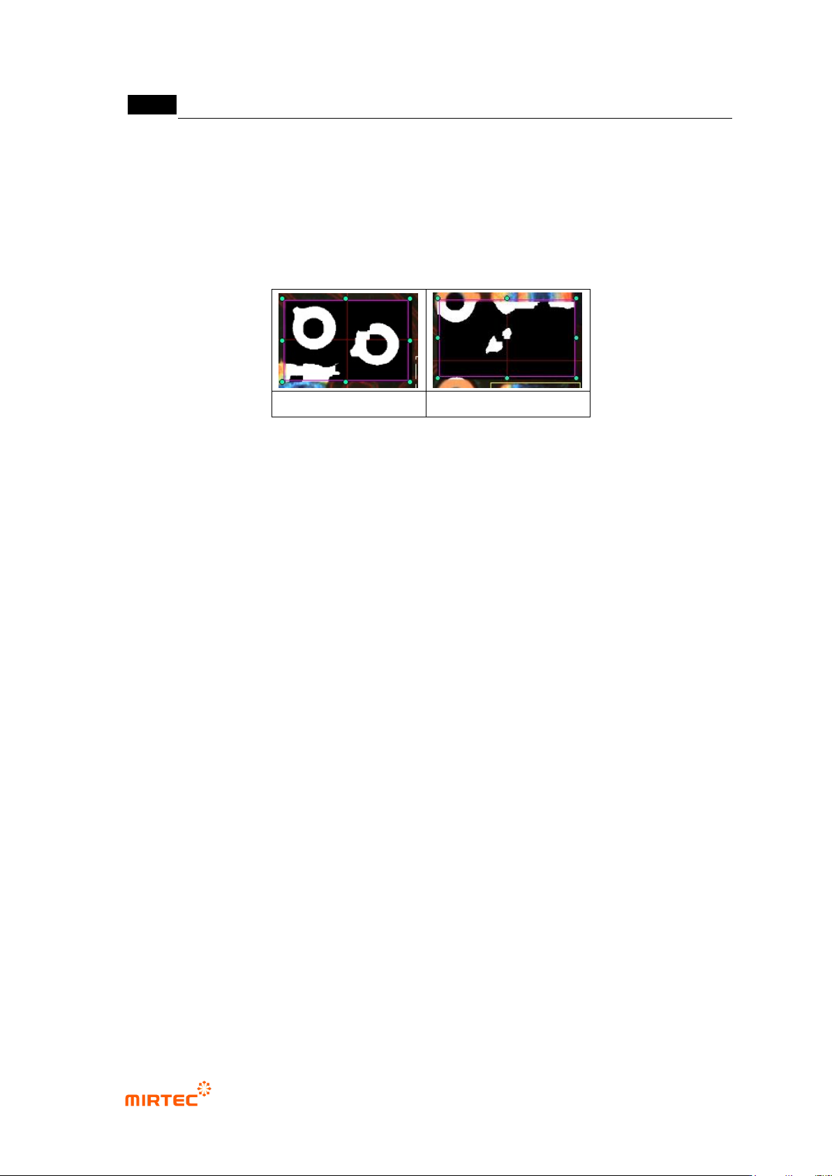
solder ball on pad
solder ball on substrate
solder ball on LED
substrate
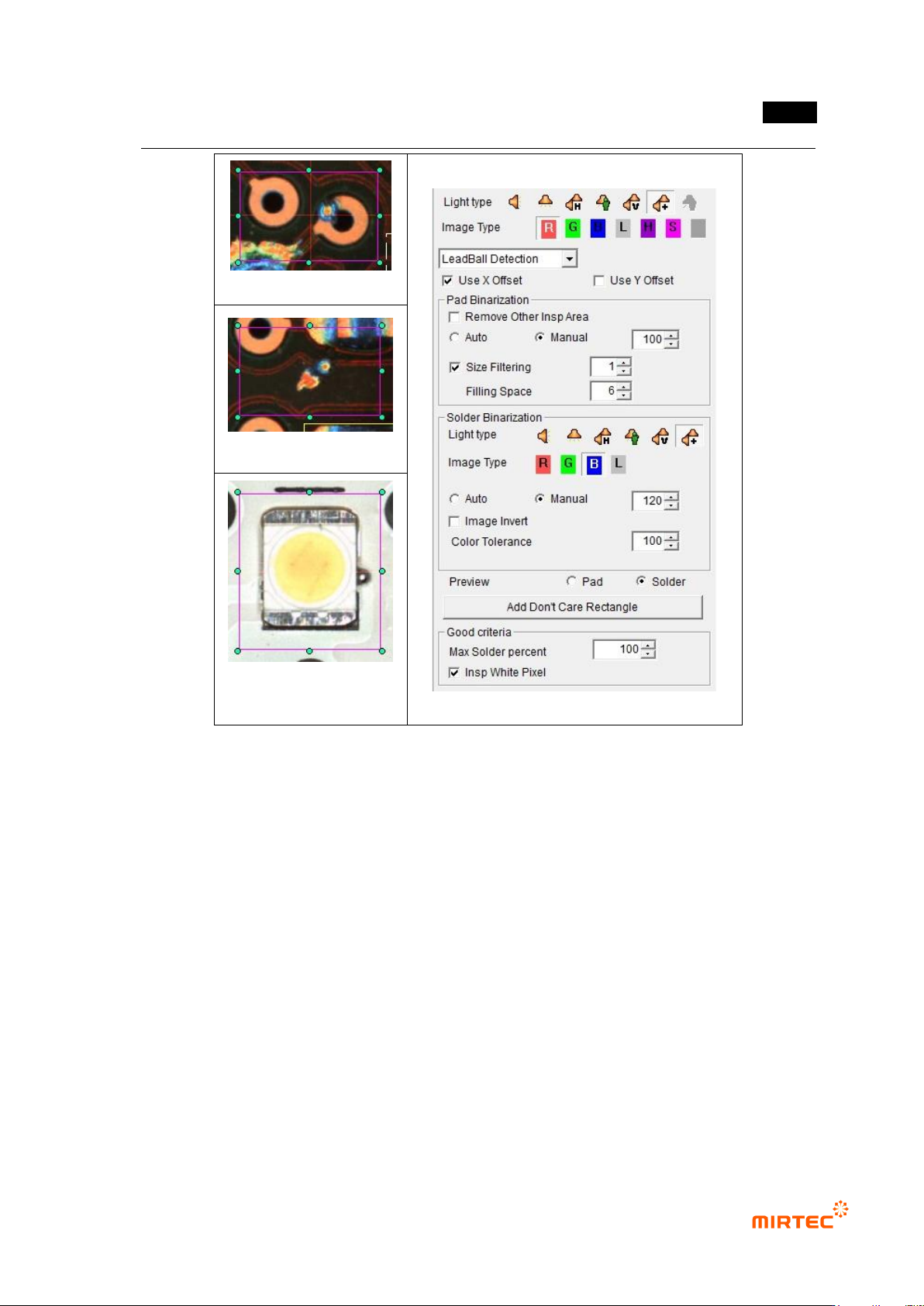
[Figure 5-85 Teaching example of solder ball inspection window]
① Parameter description
Pad/Bridge binarization
- Light type and image type
Use parameter in common parameter window for light type and image type for pad
binarization. In general, select B type or L of horizontal + vertical light. Sometimes,
select L type of vertical light.
- Exclude other inspection area
Check at this option if inspection area that completed teaching and other inspection
window is overlapped. other inspection window will be regarded as „Don‟t care
region‟.
- Binarization
Set auto or manual for binarization. Set binarization value checking preview-pad
during manual setting.
MV-9 User Manual
5-80
To detect Solder ball on LED substrate, set binarization value to „0‟ to make total
inspection window in white in preview.
- Size filtering, space filling
For detection of solder ball on pad, set binarization to low value. Set size filtering to
low value, and increase space filling to clearly display whole pad area.
To detect Solder ball on LED substrate, it‟s fine not to set it.
solder ball on pad
solder ball on substrate
[Figure 5-86 pad/Bridge binarization preview image]
Solder binarization
- Light type and image type
Select light type and image type to separate solder ball
In general, select horizontal + vertical light-B type or select horizontal light-L type.
- Binarization and color allowable value
Set binarization value and color allowable value for good separation of solder ball
checking preview-solder.
Color allowable value: setting to tell chromatic color from achromatic color. Inspect
RGB color in white area in solder binarization image to recognize difference of max
value and min value of RGB value. If the difference is above color allowable value,
in other words, in case of achromatic color, recognized as hole or scratch not solder
and excluded. The lower setting is, the most area is excluded. The higher setting is,
the smaller excluded area.
- Image reverse
This function is to reverse binarization image. set this function to detect Solder ball
on LED substrate
错误!使用“开始”选项卡将 제목 2 应用于要在此处显示的文字。错误!使用“开始”选项卡将 제목 2 应用
于要在此处显示的文字。 .
5-81
solder ball on pad
solder ball on substrate
solder ball on LED
substrate
[Figure 5-87 solder binarization preview image]
Preview
- This is to display preview image during binarization, select pad or solder.
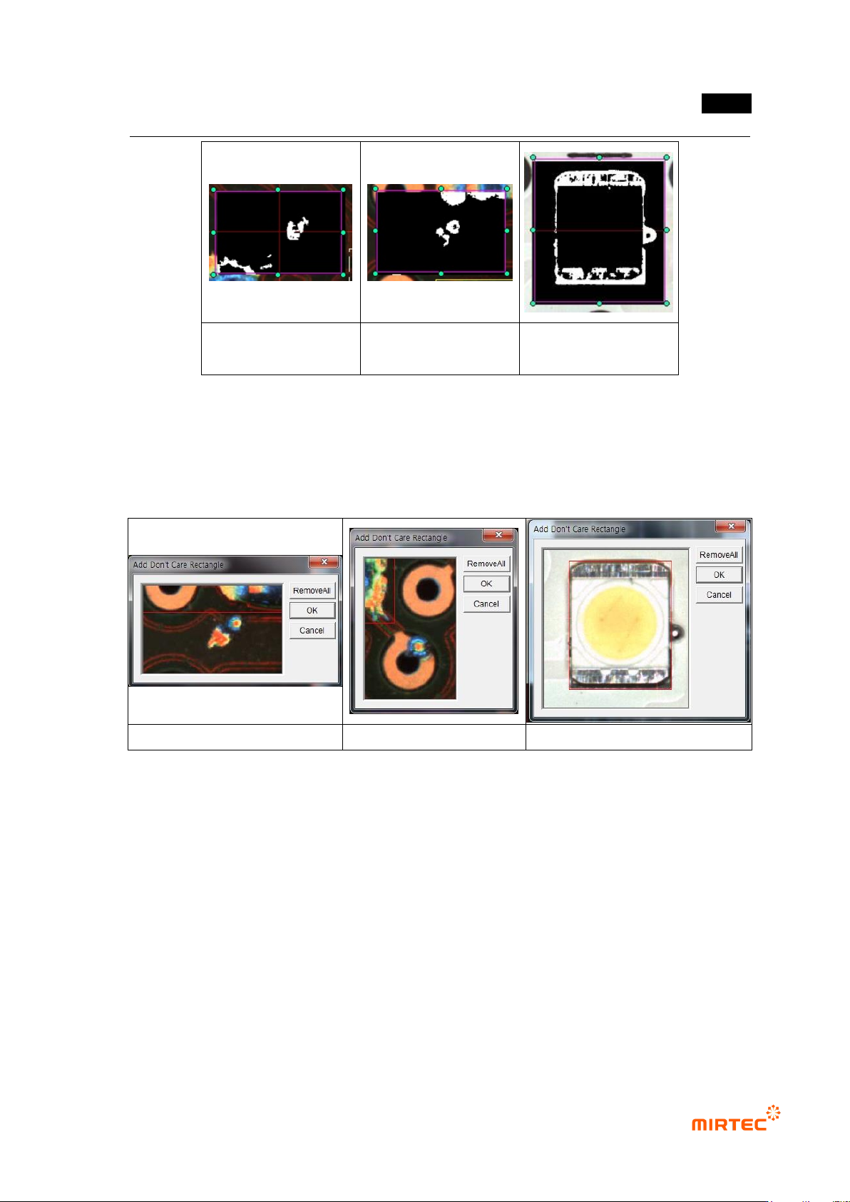
Add ‘Don’t care rectangle’
- This function is to set „Don‟t care region‟.
solder ball on pad
solder ball on substrate
solder ball on LED substrate
[Figure 5-88 Add ‘Don’t care rectangle’]
Normal criteria
- Max solder amount: Enter reference value to judge good/defect
- White pixel inspection: make good/defect judgment based on number of pixel of solder ball
area.
If white pixel inspection is checked, max solder amount is inspected based on the
number of white pixel of area that is separated by solder ball. If it is not checked,
inspected based on ratio.
Solder ball area comparing to ratio of pad area is displayed during detecting solder
ball on pad for ratio inspection. Solder ball area comparing to ratio of whole
inspection window area for detection of solder ball on substrate.