MV-9_Chapter 5. Teaching.pdf - 第47页
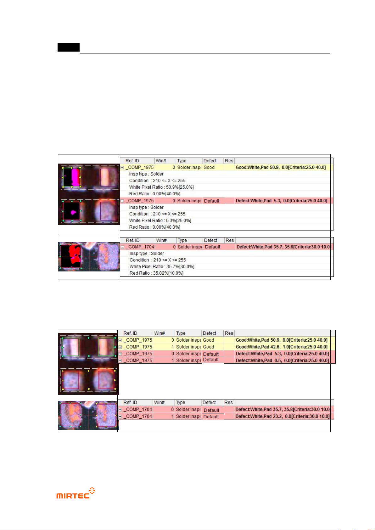
错误 ! 使用“开始” 选项卡将 제목 2 应用于要在此处显示的文字。 错误 ! 使用“开始”选项卡将 제목 2 应用 于要在此处显示的 文字。 . 5- 47 - Inspection T ype : name of inspection window . - Condi t ion : status of binarization setting. - Red Ratio : ratio of red pixel in inspec…
MV-9 User Manual
5-46
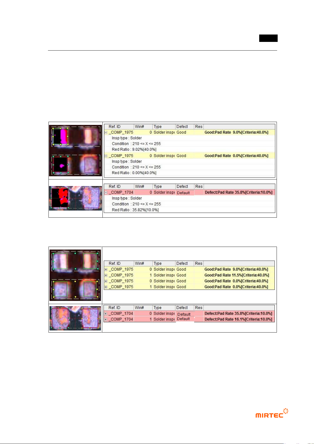
- Condition: status of binarization setting.
- White Pixel Ratio: ratio of white pixel in inspection window. It means ratio of pixel relevant
to electrode.
- Red Ratio: ratio of red pixel in inspection window. It means ratio of pixel relevant to
exposed pad.
- Non-mounting defect at which chip is not mounted and non-mounting defect at which is
mounted but sprang off can be detected while checking ion chip polar star check.
[Figure 5-48 Non-mounting inspection (mounting) in status screen –result when chip inspection
check is selected]
[Figure 5-49 Non-mounting inspection (mounting) –result example when chip inspection check is
selected]
When chip electrode check is selected
错误!使用“开始”选项卡将 제목 2 应用于要在此处显示的文字。错误!使用“开始”选项卡将 제목 2 应用
于要在此处显示的文字。 .
5-47
- Inspection Type: name of inspection window.
- Condition: status of binarization setting.
- Red Ratio: ratio of red pixel in inspection window. It means ratio of pixel relevant to
exposed pad.
- Non-mounting defect at which is mounted but sprang off can be detected if chip electrode
is not selected. However, but defect at which chip is not mounted can‟t be detected.
[Figure 5-50 Non-mounting inspection (mounting) in status screen – result when chip inspection
check is not selected]
[Figure 5-51 Non-mounting inspection (mounting) – result example when chip inspection check is
not selected]
MV-9 User Manual
5-48
5.3.3.2. Color inspection
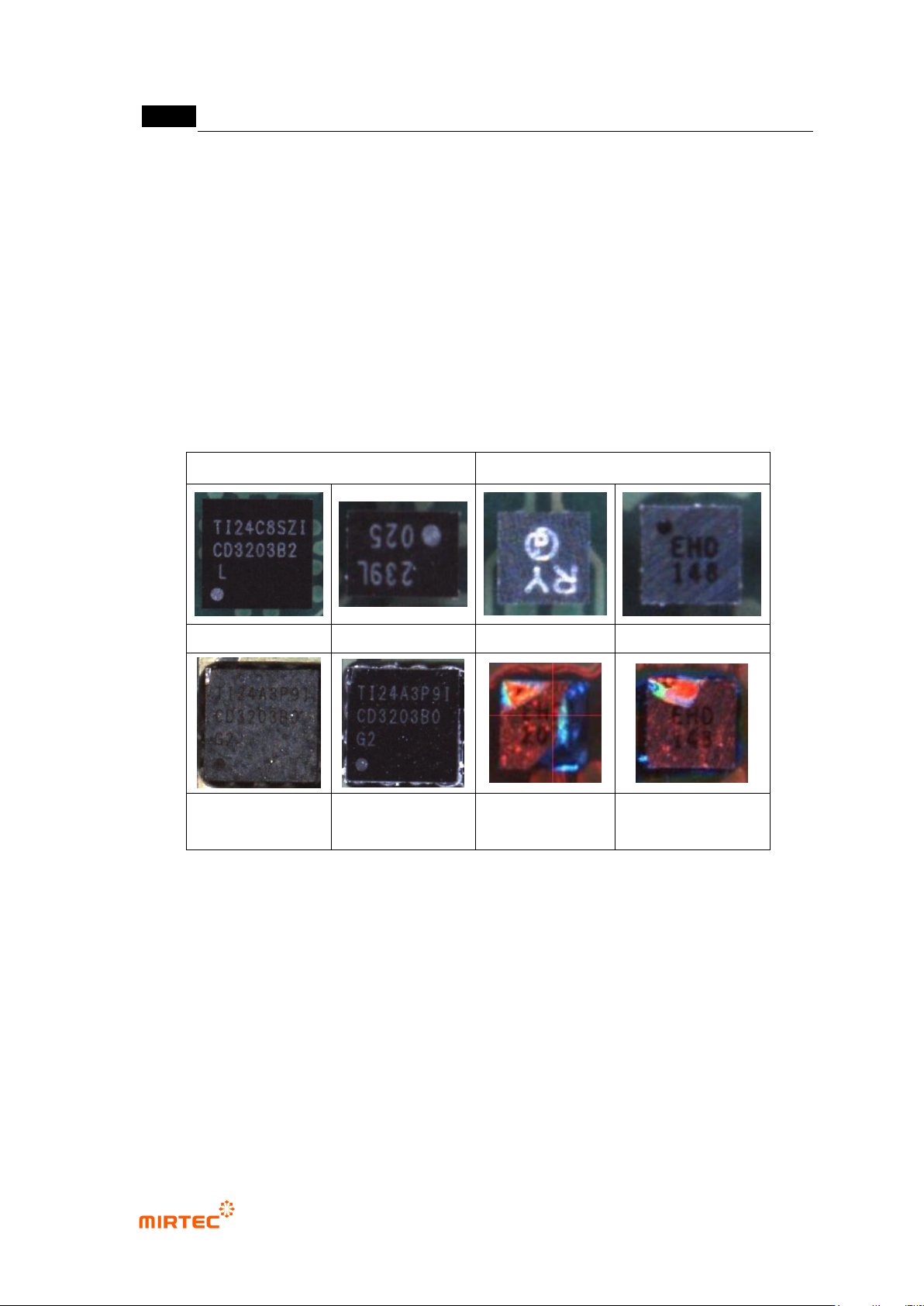
1) Crack inspection
- Crack inspection algorithm is to detect crack defect of BGA surface or other components.
- Crack characteristic
Chipping or Crack part appears relatively lighter Red or lighter Blue than normal
surface in color light and appears relatively brighter or darker than normal surface
in white light.
The figure below shows normal image and Chipping or Crack defect image.
BGA
CSP
normal
normal
normal
normal
defect – vertical light
defect - horizontal
light
defect - color light
defect - color light
[Figure 5-52 Normal image and crack defect image]
① Teaching method
(a) Draw on solder window on inspection target area of a component. In general, set whole
chip package as an inspection area.
(b) Select color inspection and select crack in component type.
(c) Select horizontal + vertical light for light type, and select A (all band = R+G+B) or L for
image type. In case of white light, use horizontal or vertical light that shows well and
select L for image type.
(d) Use color map and binarization to separate crack defect of BGA or CSP.