MV-9_Chapter 5. Teaching.pdf - 第59页
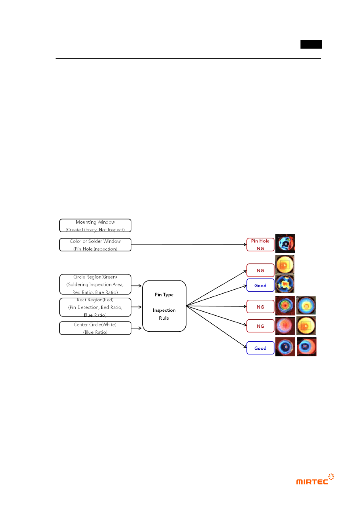
错误 ! 使用“开始” 选项卡将 제목 2 应用于要在此处显示的文字。 错误 ! 使用“开始”选项卡将 제목 2 应用 于要在此处显示的 文字。 . 5- 59 4) Good/defect judgment rule - Soldering shape of pin type is almost simila r , and most of pin e x posure can be clearl y recognized. Howe…
MV-9 User Manual
5-58
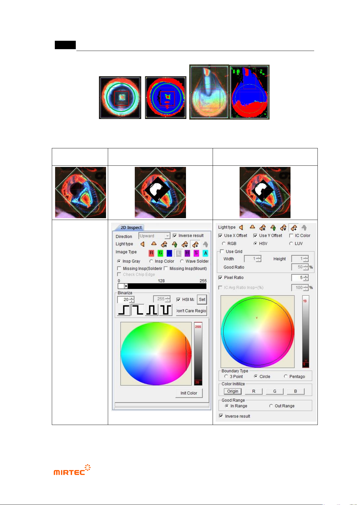
[Figure 5-62 Wave soldering inspection teaching and preview]
Normal image
Soldering inspection teaching
window
Color inspection teaching window
[Figure 5-63 perforation inspection teaching and preview]
错误!使用“开始”选项卡将 제목 2 应用于要在此处显示的文字。错误!使用“开始”选项卡将 제목 2 应用
于要在此处显示的文字。 .
5-59
4) Good/defect judgment rule
- Soldering shape of pin type is almost similar, and most of pin exposure can be clearly
recognized. However, soldering shapes of lead type are very various according to lead
amount, and many times image does not displayed according to bending angle of lead
even in normal soldering status. Hence, use a lot of information for more correct inspection
and good/defect judgment.
Pin type inspection sequence
Perforation inspection will be independently conducted in color inspection window.
For multi-pin type, no solder, inspect insufficient solder, excessive solder defect using
blue ratio in soldering inspection area and red ratio in pin (lead) inspection area.
For pin type, inspect no solder, insufficient solder, excessive solder and no pin exposure
defect using red ratio in pin (lead) inspection area and blue ratio in excessive solder
inspection area according to blue ratio of soldering inspection area.
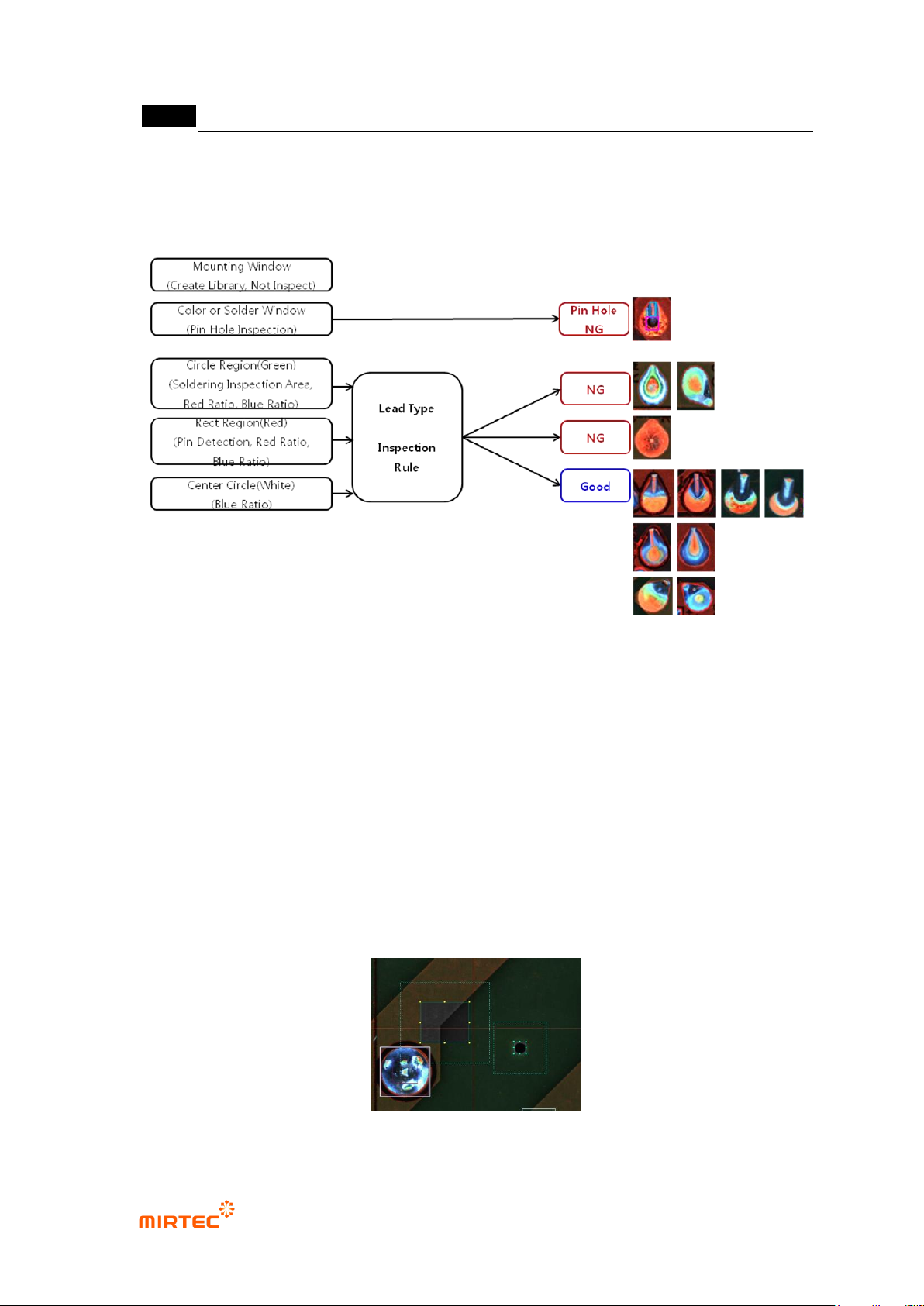
Lead type inspection sequence
Perforation inspection will be independently conducted in color inspection window.
In case of lead type, if lead is exposed, judge as good. Exposed lead appears in red in
color image. However, in many cases, lead does not appeared in red by bending angle
of lead and lead amount in normal soldering status.
Red ratio in pin (lead) inspection area is larger than reference value. Judge good/defect
using blue ratio and red ratio in soldering inspection area.
MV-9 User Manual
5-60
In case red ratio in pin (lead) inspection area is smaller than reference value, inspect
insufficient solder, excessive solder and no pin exposure defect using shape of red area
in soldering inspection area, blue ratio in excessive solder inspection area.
5) Teaching guide
Use frame compensation mark
- There are many wave soldering surface statuses, and we have to register many sample
images to use mounting inspection.
- Characteristic of high position precision (pattern, through hole, etc) is used for frame
compensation mark. Through hole sometimes blocked by solder. Hence, we set both of the
first and second.
- Select color light, and select type that has lowest noise value for image type. (In general, L
type)
- Considering there is much flux on substrate surface due to characteristic of wave soldering,
selection of horizontal light shows the best display. However, use color image for
inspection speed if it‟s possible.
[Figure 5-64 Setting example of frame compensation mark]