MV-9_Chapter 5. Teaching.pdf - 第37页
错误 ! 使用“开始” 选项卡将 제목 2 应用于要在此处显示的文字。 错误 ! 使用“开始”选项卡将 제목 2 应用 于要在此处显示的 文字。 . 5- 37 - Since soldering area i s slope on PCB, ligh t ty pe of hor i zonta l + ver t i cal li ght ( ) and image type of B (blue) for slope area a…
MV-9 User Manual
5-36
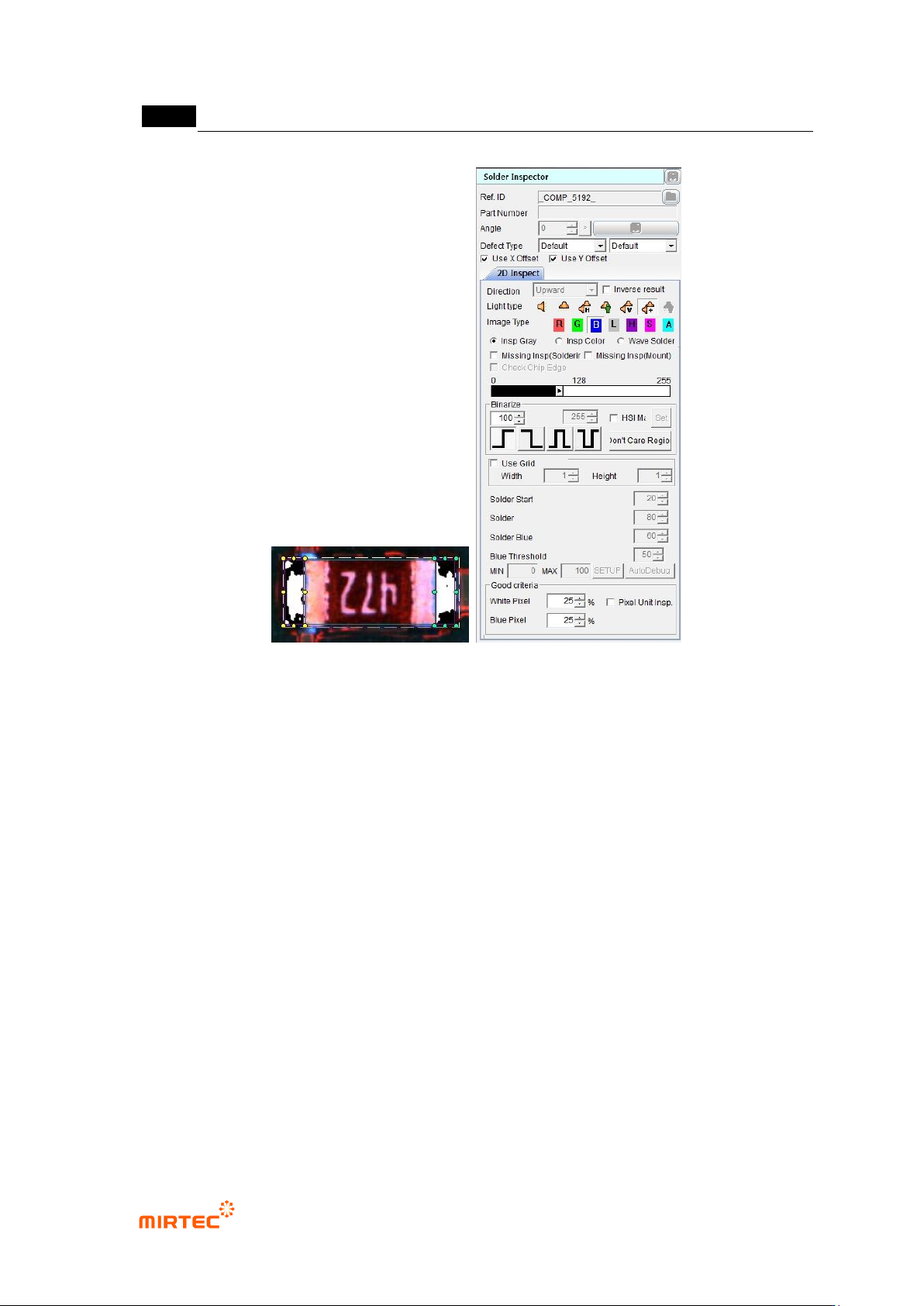
[Figure 5-37 Screen to create soldering inspection (basic) window]
② Parameter of soldering inspection (basic) window
Reference name
- Refer to „reference name (page5-21) ' in „5.3.1 mounting inspection window‟‟ excepting
shape.
- Created in „_SLD_1_‟ format. „SLD‟ means Solder and number means creation order of
solder amount inspection window.
Component name
- Refer to „component name‟ in '5.3.1 mounting inspection window‟‟.
Rotation angle
- Refer to „rotation angle‟ in '5.3.1 mounting inspection window‟‟.
Defect type
- Refer to „defect type‟ in '5.3.1 mounting inspection window‟.
Light type
- Select light type and image type in which soldering area of component is clear.
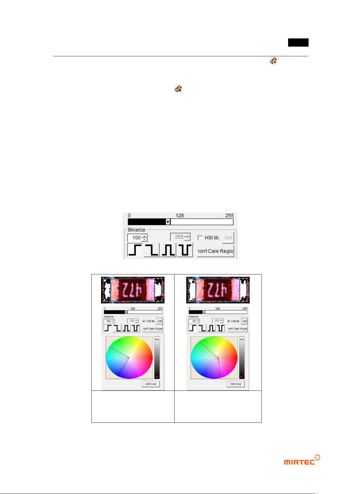
错误!使用“开始”选项卡将 제목 2 应用于要在此处显示的文字。错误!使用“开始”选项卡将 제목 2 应用
于要在此处显示的文字。 .
5-37
- Since soldering area is slope on PCB, light type of horizontal + vertical light ( ) and
image type of B (blue) for slope area are recommended. L (luminance) can be also
selected.
- If necessary, select horizontal - vertical ( ) or L (luminance). Vertical white light and
horizontal white light are used to create horizontal - vertical image.
Image type
- In case of horizontal + vertical light, select B or L for image type. In case of horizontal -
vertical, select L for image type.
Binarization
- This means to express images in white (1) and black (0) for black and white image that is
express by 256 steps based on specific level value(binarization value).
- User can adjust desired color, saturation and luminance area for image type selected
using color map.
- To check binarized image in frame image screen, click <preview> button in „operating
buttons‟. [Table5-3] shows 4 binarization methods.
[Figure 5-38 Binarization value setting]
Binarization image in initial
status of color map
Binarization image after
adjusting color map and
binarization
[Figure 5-39 Binarization value setting]
MV-9 User Manual
5-38
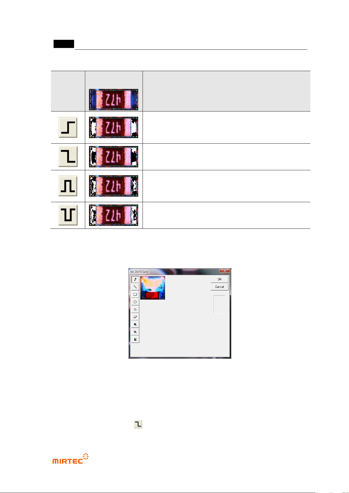
[Table 5-3 4 Binarization methods of solder inspection window]
Status
Binarization
image
Description
Horizontal + vertical light image
binarize all level value below reference to black (0), and all
level value over reference to white (1) based on one
binarization value (Ex: 100)
Binarize all level value below reference to white (1), and all
level value over reference to black (0) based on one
binarization value (Ex: 100).
Binarize all level value within reference range to white (1),
and all level value beyond range to black (0) based on2
binarization value (Ex: 100, 150).
Binarize all level value within reference range to black (0),
and all level value beyond range to white (1) based on2
binarization value (Ex: 100, 150).
‘Don’t care region’
- We can set „Don‟t care region‟ by drawing area in image in inspection window.
[Figure 5-40 ‘Don’t care region’ setting screen]
Use grid inspection
- Divide solder inspection window with grid and individually inspect each area to detect
solder ball or foreign material on pad.
- Since foreign material on a pad is brighter than pad in horizontal + vertical light, select B or
L for image type, select for binarization method, and adjust binarization value.