MV-9_Chapter 5. Teaching.pdf - 第116页
MV -9 Use r Manual 5-1 1 6 [Figure 5- 127 stripe wid th example] Noise removal – a rea This option is used t o r em ove noi se com pon ent that has value below area (pixel region) set in binarized im age . (Ex: use d…
错误!使用“开始”选项卡将 제목 2 应用于要在此处显示的文字。错误!使用“开始”选项卡将 제목 2 应用
于要在此处显示的文字。 .
5-115
Set whether IC/Bridge inspection window conducts solder amount inspection for fillet part
or not. „Lead tip‟ tap and „solder amount inspection‟ tap will be activated when this option
is set.
Direction
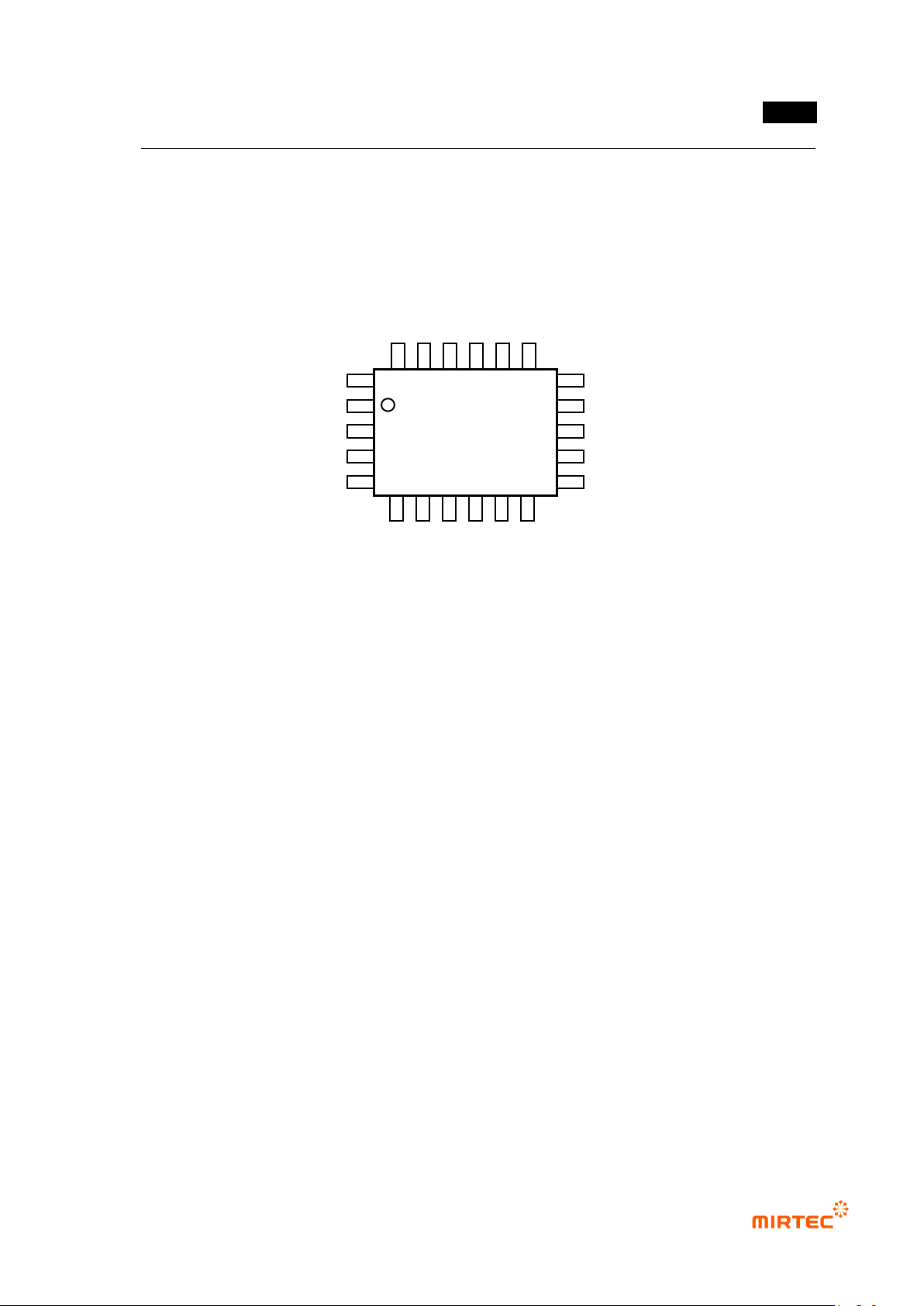
Direction of lead spread based on IC component body.
[Figure 5-126 IC component shape]
IC color
Check at this function for lifted lead inspection by interlocking color inspection window
with IC Bridge inspection window.
For normal range for IC color inspection, set it using pixel ratio (upper limit) and IC
average ratio inspection+ (%) (lowest limit) in color inspection window.
9) Common parameter
For smooth conduction of the relevant inspection or area setting, there are items to
adjust parameter on each tap. The followings are parameters commonly used on each
tap.
Binarization boundary value
Auto: program automatically set binarization value for image binarization.
Manual: users directly set binarization value for image binarization.
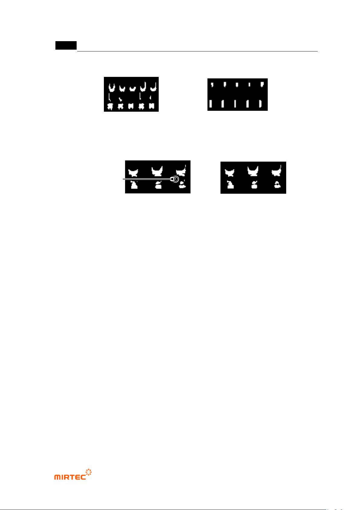
Noise removal – stripe width (Pass Stripe)
This is used to remove length direction noise component of lead from binarized image.
The larger value, the thinner lead width.
Upward
Rightward
Leftward
Downward
MV-9 User Manual
5-116
[Figure 5-127 stripe width example]
Noise removal – area
This option is used to remove noise component that has value below area (pixel region)
set in binarized image. (Ex: used to detect „solder ball‟ defect between lead and lead.)
[Figure 5-128 Small area removal example]
Fix edge
Use this option to reduce false defect due to silk when bridge position pushed to exterior
by compensation window during bridge inspection.
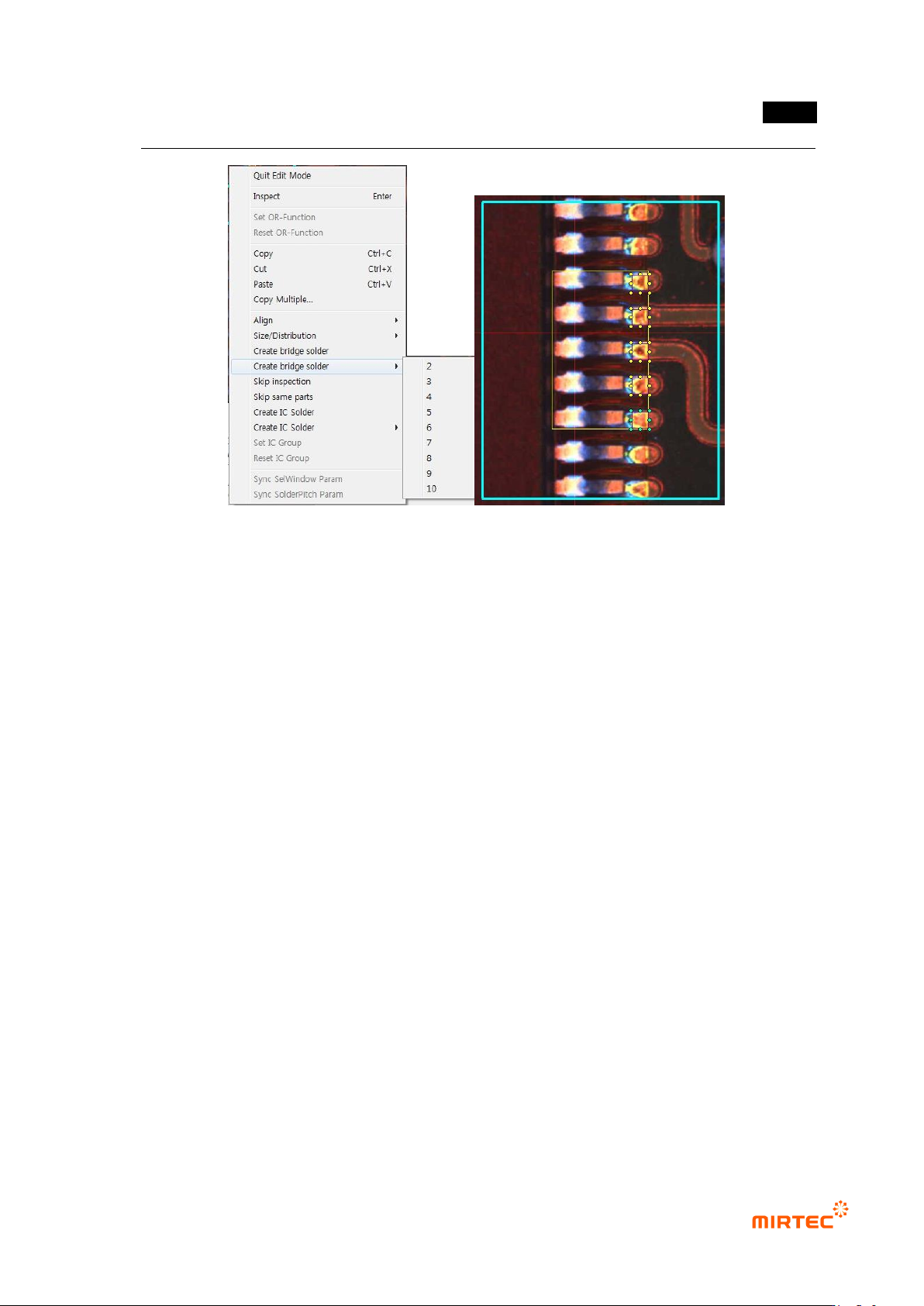
Use solder pitch
Use lead separation information (average lead pitch) and add bridge solder to conduct
soldering inspection of fillet area.
Adding of bridge solder is possible only in edit mode, select IC Bridge inspection window,
and select „Add Bridge solder‟ in popup menu (click the right button of a mouse) to
automatically create solder inspection window.
lead separation tap is not activated. If comparison inspection is not checked, lead tip tap
and lead amount inspection tap will not be activated. However, solder amount inspection
function will be activated if comparison inspection is checked.
Small area removal - 0
Small area removal - 60
Small area removal
stripe width: 0
stripe width: 6
错误!使用“开始”选项卡将 제목 2 应用于要在此处显示的文字。错误!使用“开始”选项卡将 제목 2 应用
于要在此处显示的文字。 .
5-117
[Figure 5-129 Bridge solder add example]
Comparison inspection
this function is to prevent occurrence of false defect when soldering status is normal but
lead amount is relatively small and white pixel ratio in solder inspection area is below
normal criteria.
For solder amount inspection, compare lead judged as defect with amount average value
of all lead, and compare it with the amount of adjacent lead.
If lifted inspection is set, lifted inspection will conduct same comparison inspection for
defective lead.
Default light
Click light change tap on the bottom of frame image screen to change light change to
change frame image. In general, currently selected light is set to light in inspection
window while drawing inspection window. (mounting, solder, binary, etc)
In case of IC/Bridge inspection window, light for each setting parameter tap can be set.
Only light in Bridge tap is et as the current frame image light and light in other taps
remains previous light.
10) Lead separation parameter
For lead separation parameter, adjust parameter for good division of lead part in preview
image. In general, select R for image type in horizontal + vertical light, and use high
binarization value and stripe width.